
Project Assistant Professor at the Institute of Engineering Innovation, Graduate School of Engineering, the University of Tokyo.
Q1. What made you decide to become a researcher?
A1. An interest in the science of everyday "things" allowed me to indulge my hobby of photography.
Impressed by the fact that there was actually profound scientific basis to the materials used for fabricating everyday "things," I decided to pursue a career in materials engineering. Later, when choosing a laboratory, we talked about my hobby of photography, and it was recommended that "if that's the case, you'll love research here." It was at this laboratory that I had my first encounter with the process of electron microscopy, which is also my current specialty.
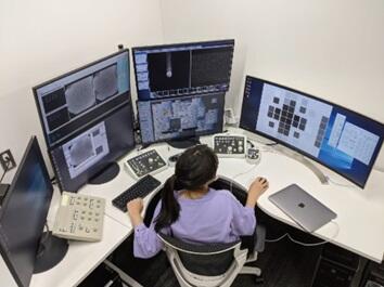
Unlike optical microscopes, which magnify an object by exposing it to visible light, electron microscopes, as the name implies, use an electron beam for observation. Among such microscopes, a scanning transmission electron microscope (STEM) allows extremely fine observation at the scale of 0.1 nanometers (nano is one billionth of a meter). I became increasingly involved in STEM research, partly because my fascination with being able to see things that were previously invisible by carefully adjusting certain conditions had something in common with my hobby of photography using an optical camera.
Q2. What are you working on in STEM?
A2. Measurement of electric and magnetic fields at the material interface, and local strain analysis in structures.
In the ERATO Shibata Project, we are developing a method for observing local electromagnetic fields in materials at high resolution using STEM. Attempts are currently being made to control the electromagnetic field and charge distribution below the nanoscale to improve the properties of materials. However, measuring such a small area is very difficult, and until now, analogies have relied on the average information over a larger area. If we can measure the local electromagnetic field and charge at the interface, simultaneously with the measurement of the atomic structure, at the nanoscale or at smaller scales, we can use the information obtained to manufacture semiconductor devices and other products.
Recently, we achieved direct observation and quantification of a two-dimensional electron gas (2DEG) localized at the hetero-interface of gallium nitride semiconductors using magnetic field-free atomic resolution STEM (MARS). Although 2DEGs are important elements of semiconductor devices, their local observation by STEM has been difficult due to the large influence of the strain present in samples. Therefore, we developed a method for effectively reducing the effects of strain and performed analyses. The process of seeing something that had never been seen before with a new method presented many difficulties. However, I was able to create an "eye" capable of directly observing the distribution of a 2DEG, which, previously, could only be approximated based on theoretical calculations and indirect measurements. I feel it was a significant contribution to the development of electron microscopes and manufacturing as well as a great boost to my own life.
Q3. What are your goals for the future and what advice do you have for future researchers?
A3. I want to find and study new physical phenomena. I hope you enjoy your own research.
In the history of mankind, the invention of the telescope and microscope contributed greatly to the advancement of science and technology. The ability to observe what was previously invisible presents an opportunity for humanity to expand its world. From now on, I would like to dedicate myself to collaborative research and development endeavors with microscope manufacturers and device development engineers. In future, I would like to try to discover new physical phenomena by capturing hitherto unseen electromagnetic field structures.
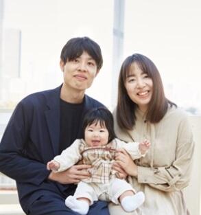
Now that I have a child, I am conscious of gathering information and engaging in trial and error with the time available in my public and private life. I know that when you first start research, you may have a vague sense of purpose, and it can be difficult, but the research that you do and output on your own brings a different dimension of joy compared to the input-driven study you have been doing. I hope that all students will absorb both their successes and failures and enjoy their unique research.
TEXT: Manami Yokoi

Profile
Satoko Toyama
Project Assistant Professor at the Institute of Engineering Innovation, Graduate School of Engineering, the University of Tokyo.
Born in Kanagawa Prefecture, Japan. Graduated from the Graduate School of Engineering, the University of Tokyo in 2023. PhD in Engineering. She has been a researcher for the "SHIBATA Ultra-atomic Resolution Electron Microscopy Project" of ERATO since the same year.