
A group at the Kyoto University's Faculty of Engineering comprising Soobeom Lee, a Ph.D. student (currently a researcher at the same university), and Professor Masashi Shiraishi collaborated with TDK and Osaka University to discover novel spin-orbit interaction (SOI) properties that go beyond the conventional understanding of the physical properties of silicon.
Silicon semiconductors using spin are expected to be used as next-generation semiconductors, however, a bottleneck in their implementation is the requirement of an external magnetic field. In this study, the research group successfully manipulated the spin flowing through silicon without using an external magnetic field. Professor Shiraishi said, "By optimizing the oxide film as a material with a high dielectric constant, its operability can be improved by approximately two orders of magnitude. I want to work toward its practical use." These findings were published in the journal, Nature Materials.
Silicon-based integrated circuits enable low-power consumption and high-speed operation through miniaturization of complementary metal-oxide-semiconductor (CMOS) transistors; however, they are approaching the limits of miniaturization. An innovative device that can fundamentally solve this problem is a spin metal-oxide-semiconductor field-effect transistor (MOSFET) that utilizes the spin degree of freedom of electrons as an information carrier. The spin MOSFET is a new type of device that uses a magnetic material for the electrodes and has both memory and transistor functions in one device simultaneously. It is expected to realize nonvolatile memory function and high-speed operation with high integration potential and high repeating memory resistance. In particular, the silicon in this MOSFET is almost inexhaustible, and the spin is expected to be retained for a relatively long time. Furthermore, the accumulated technical and infrastructural aspects of conventional silicon electronics mean that research has been actively conducted since 2007 to realize spin MOSFETs using silicon worldwide.
The joint research group succeeded in operating a silicon spin MOSFET at room temperature for the first time in the world in 2014 and succeeded in significantly improving its performance in 2016. An external magnetic field is used to operate the spin. However, the information computing element must be as compact as possible. Having a separate function to apply an external magnetic field prevents compaction of this element. To improve this aspect of the device, research on manipulating spins by artificially generating an effective magnetic field in matter through SOI has been conducted extensively. When this effect is used, it is not necessary to apply an external magnetic field. Therefore, the information element can be made significantly more compact.
One large issue is that it has been considered impossible, in principle, to generate an effective magnetic field through SOI with silicon and equip it with a spin manipulation function. As the magnitude of spin-orbit interaction is approximately proportional to the fourth power of the atomic number, silicon with an atomic number of 14 can essentially exhibit only small SOI. In addition, this SOI occurs in substances with low inversion symmetry. However, silicon has a high inversion symmetry, and SOI cannot be expressed significantly due to this as well. Due to these properties, the research group focused on the structure of silicon spin MOSFETs.
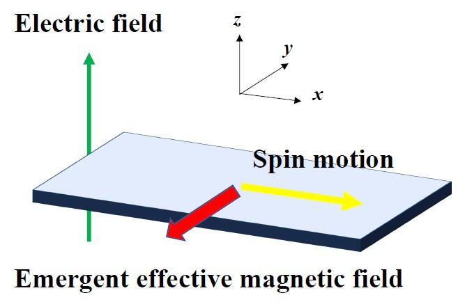
Another approach to expressing spin-orbit interaction is using the internal electric field (Rashba field) generated at the junction (interface) of two substances and the velocities of the electric field applied from the outside and the electron carrying the spin. According to the special theory of relativity, when a substance moves very quickly, an effective magnetic field spontaneously emerges in a direction perpendicular to both the direction of motion of the substance and the direction of the electric field. The idea is to manipulate the spins moving in silicon by applying this effective magnetic field without the need for an external magnetic field. Professor Shiraishi said, "While analyzing experimental data, we believed that some parts could not be explained by conventional theory. When we examined them by changing the analysis method in 2014, we found that the silicon oxide layer would worsen the symmetry; therefore, it may be possible to operate these devices with the gate voltage."
Credit: Kyoto University
In their experiments, the research group used the Rashba field. This field is an internal electric field; it is expected to exist at the interface of a 100-nm-thick silicon layer, which is the spin-carrying layer of a silicon spin MOSFET, and the silicon oxide layer immediately below it. Furthermore, electric fields of 10, 60, and 100 V were applied through this silicon oxide layer. At 60 V or higher, a magnetic field was artificially created in the silicon, and the spin flowing through the silicon was manipulated successfully. They also succeeded in completely extinguishing the Rashba field by tuning the external electric field, demonstrating that the spin information flowing through silicon can be manipulated easily. This finding signifies that the study has gone beyond the conventional understanding of physical spin characteristics regarding silicon (i.e., because silicon exhibits essentially no spin-orbit interaction, an external magnetic field must be used to manipulate the spin information flowing inside). The results demonstrated that the spin information flowing through silicon could be manipulated only by an electric field without applying any external magnetic field.
This provides a new perspective on developing silicon spin information devices using silicon spin MOSFETs. The development of these devices is expected to further accelerate. However, in these experiments, the degree of spin information manipulation was up to 30%, which is not sufficiently efficient for practical applications. The research group will work towards developing methods for applying a stronger electric field more efficiently and optimize the device structure in the future.
This article has been translated by JST with permission from The Science News Ltd.(https://sci-news.co.jp/). Unauthorized reproduction of the article and photographs is prohibited.