
The research group, which includes Invited Researcher Ryota Negishi (currently Associate Professor of Toyo University Faculty of Science and Engineering), Professor Yoshihiro Kobayashi, Professor Nobuya Mori of the Osaka University Graduate School of Engineering, and Professor Hirofumi Tanaka of the Kyushu Institute of Technology Graduate School of Life Science and Systems Engineering/Research Center for Neuromorphic AI Hardware, has succeeded in clarifying the mechanism of generation of metallic and semiconductor characteristics in a graphene nanoribbon (GNR) by analyzing the carrier transport properties of electric field effect transistors (FET) using multi-layer graphene nanoribbon as a channel.
The research group has pioneered a crystal growth method for forming a new graphene layer on a two-dimensional graphene sheet, which has the same carbon six-membered ring structure as GNR. By applying this technology, they attempted to form a multi-layer GNR structure.
GNR is a one-dimensional nanocarbon material in the shape of a ribbon (thin wire), and its width is on the scale of a few nanometers. Since crystal growth similar to that of macroscale graphene is performed on such nanostructures, a multi-layer GNR was formed by optimizing many growth conditions such as the amount of carbon source gas, temperature, and gas flow rate.
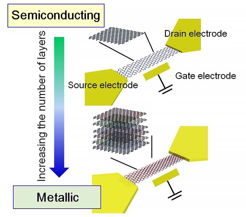
While controlling the width of this multi-layer GNR to 15 to 25 nm, the carrier transport properties in the FET using a multi-layer GNR channel with different numbers of layers was measured. Semiconductor-like properties were observed in graphene with a small number layers (1 to 3 layers), and metallic properties were observed with multiple layers (6 to 8 layers) as the effect of the impurity charge on the device substrate, silicon oxide surface (SiO2 / Si), was reduced. Semiconductor transistors that are several tens of nanometers in size have supported the development of today's information and communication society. However, at this extreme scale, the development of alternative materials is becoming prevalent worldwide because the principle limit at which semiconductor transistors do not work has been reached.
Credit: Osaka University
Researcher Negishi said, "This study has clarified the design guidelines for GNRs that incorporate actual device structures. In the future, we would like to develop scalable formation technology such as arraying of multi-layer GNR structures designed according to their purpose, e.g., high speed transistors and ultra-thin wiring."
This article has been translated by JST with permission from The Science News Ltd.(https://sci-news.co.jp/). Unauthorized reproduction of the article and photographs is prohibited.