
As part of the "Development of Technologies for Super Energy-Efficient Optical Electronics Implementation Systems" project promoted by the New Energy and Industrial Technology Development Organization (NEDO), the Photonics Electronics Technology Research Association (PETRA) developed the world's first LSI circuit using a transistor with ultra-low power consumption. The prototype sample transmitted the next-generation standard 112 Gbps (gigabit/second) optical signal in a high-temperature (over 80 °C) environment, demonstrating its usefulness. By utilizing 3D optical wiring technology, integration is possible with the distance of electrical wiring in the LSI integrated circuits shortened to the utmost limit. Therefore, a significant reduction in power consumption, about 30-40%, is expected compared with conventional technology. PETRA presented this achievement at the Optoelectronics and Communications Conference (OECC) 2021, one of Asia's largest international conferences on optical communications, held from July 3rd to 7th.
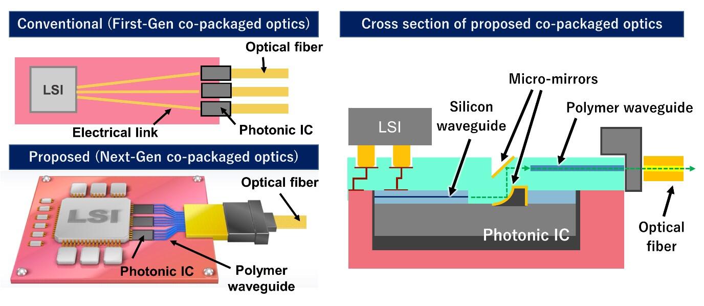
The cross-sectional area of light passing through the optical fiber (waveguide) differs by more than 10 times between the silicon and the polymer components that constitute the photonic IC. In addition, as the refractive indices of the two components are significantly different, substantial light loss will occur if they are connected as they are in the communication wavelength band. Therefore, a technology for converting the shape of the beam of light was required for the connection.
By creating an aspherical mirror on the substrate that reflects the output light from the silicon optical waveguide in the vertical direction, the beam diameter of the light can be optimally controlled and used in combination with the upper 45° mirror. This has enabled the development of a micromirror that uses 3D optical wiring technology to connect to a polymer optical waveguide after freely controlling the light path in three dimensions. However, as the developed 3D micromirror uses silicon and a polymer with coefficients of thermal expansion that differ by two orders of magnitude, there were concerns regarding its impact on high-temperature operation. In addition, in high-speed optical signals, the waveform may deteriorate due to multiple reflections among silicon optical waveguides, micromirrors, and polymer optical waveguides. Therefore, the researchers verified the operation of this micromirror using high-speed optical signals at high temperatures.
Credit: Photonics Electronics Technology Research Association (PETRA)
First, an optical signal with a transmission rate of 112 Gbps per channel was optically transmitted to the prototype sample at 25 °C using the Pulse Amplitude Modulation 4-level (PAM4) method, which is also envisioned as the next-generation standard for co-packaged optics. It was then confirmed that no deterioration in the signal waveform had occurred. Subsequently, demonstrations at a high temperature of 85 °C were also conducted, as required for data center operation, and it was confirmed that optical transmission could be performed without a noticeable deterioration in the signal waveform. Thus, the effectiveness of the developed next-generation co-package was demonstrated.
In the future, PETRA will utilize the results of this project to implement optical circuits in data centers and computers and realize high-speed information transmission with low power consumption between LSI circuits. PETRA will also consider multichannel and wavelength-division multiplexing and will proceed with the development of an integrated technology for LSI and photonic ICs as well as with research and development for a co-package capable of processing 50 Tbps (terabit/second). The ultimate aim is to reduce power consumption significantly by realizing optical transmission of signals in the CPU and server of data centers.
This article has been translated by JST with permission from The Science News Ltd.(https://sci-news.co.jp/). Unauthorized reproduction of the article and photographs is prohibited.