
The collaborative research group, including Associate Professor Takayuki Iwasaki and Professor Mutsuko Hatano of the Department of Electrical and Electronic Engineering, School of Engineering, Tokyo Institute of Technology; and Senior Researcher Hiromitsu Kato and Research Team Leader Toshiharu Makino of Advanced Power Electronics Research Center, National Institute of Advanced Industrial Science and Technology, succeeded in electrically detecting the spin information of the nitrogen vacancy (NV) center in diamond, which functions as a quantum sensor, using a diamond device.
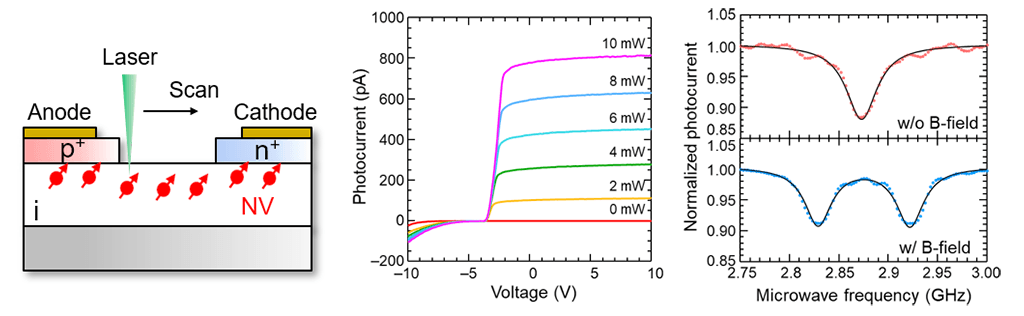
The NV center in diamond functions as a quantum sensor that can detect weak magnetic fields, such as bio magnetic fields. Normally, the fluorescence emitted by the NV center is measured using a photodetector. However, it is difficult to achieve both performance improvement and integration owing to the signal attenuation caused by optical elements and the increase in size due to an increase in the number of elements. The research group demonstrated the electrical detection technology of the NV center using the horizontal diamond p-i-n diode* semiconductor structure. The developed diamond p-i-n diode has a structure in which p-layers and n-layers, which are heavily doped with impurities via chemical vapor deposition, are patterned on the i-layer. The NV center was formed in the i-layer via nitrogen ion implantation.
As a result, it was observed that the optical carriers generated from the NV center near the p-layer via photoexcitation by the laser could be measured even when no external voltage was applied. In addition, when light of 0 to 10 mW was irradiated, a photocurrent corresponding to the power of the irradiated light was obtained. Consequently, the research group succeeded in photocurrent-detected magnetic resonance (PDMR) measurements, which electrically detect spin information from the NV center while applying microwaves. They demonstrated that the NV center functions as a quantum sensor. This finding is important in the design of solid-state quantum sensor integration.
Credit: Courtesy of AIST, Tokyo Institute of Technology. T. Murooka, M. Shiigai, Y. Hironaka, T. Tsuji, B. Yang, T. M. Hoang, K. Suda, K. Mizuno, H. Kato, T. Makino, M. Ogura, S. Yamasaki, M. Hatano, and T. Iwasaki: Photoelectrical detection of nitrogen-vacancy centers by utilizing diamond lateral p-i-n diodes, Appl. Phys. Lett. 118, 253502 (2021)
Associate Professor Iwasaki said, "The NV center of diamond functions as a quantum sensor that can detect weak magnetic fields, such as bio magnetic fields. Normally, magnetic field detection measures the fluorescence emitted by the NV center, but an electrical detection method is important for future integration. Compared with the structure used for electrical detection in the past, by combining diamond semiconductor device technology and quantum sensors, we have succeeded in electrical detection with a device that can be developed into a more sensitive and compact sensor system. By using the avalanche effect with the developed p-i-n diode, we can expect a significant increase in the signal from the NV center, which will lead to the realization of a compact and integrated quantum sensor."
* Diamond p-i-n diode: A diode made from a diamond semiconductor The p-layer is doped with boron as an acceptor, and the n-layer is doped with phosphorus as a donor. The i-layer sandwiched between the two layers is a semiconductor layer with a low impurity concentration.
■ Avalanche effect: A phenomenon in which carriers in a semiconductor accelerated by an electric field generate new carriers due to collision, and the number of carriers is amplified by repetition.
This article has been translated by JST with permission from The Science News Ltd.(https://sci-news.co.jp/). Unauthorized reproduction of the article and photographs is prohibited.