
When a high-density charge is injected into an insulating solid material without impurities, it is transformed from an insulator to a metal. However, the insulator-metal transition in organic semiconductors has not been experimentally demonstrated in the last 20 years.
A study group including Doctoral Student Naotaka Kasuya, Associate Professor Shunichiro Watanabe (concurrently serving at AIST at the time of the study) and Professor Junichi Takeya (concurrently serving at NIMS at the time of the study) and others at the Graduate School of Frontier Sciences, The University of Tokyo have developed an organic semiconductor single-crystal thin film of single molecule thickness, injected a charge into it at a high density, formed a two-dimensional hole gas state, and successfully observed the insulator-metal transition of organic semiconductors for the first time in the world. The demonstration of insulator-metal transition in organic semiconductors is expected to accelerate its application to high-speed electronic devices and quantum electronics in addition to basic research on electronic phase transitions. The group's result was published in Nature Materials.
It is known that injecting electrons and electron-holes at a high density into an insulating solid material without impurities enables its transition from an insulator that does not conduct electricity to a metal that does. This insulator-metal transition is an electronic phase transition in solid materials and has been studied extensively for a long time. Insulator-metal transitions have also been studied in organic semiconductor crystals with semiconductor-like properties but have not yet been demonstrated experimentally. This is because it was difficult to produce extremely high-purity organic semiconductor thin films without defects. Organic semiconductor crystals are also susceptible to external disturbances because they are held together only by weak intermolecular forces, making it difficult to inject charges at high densities.
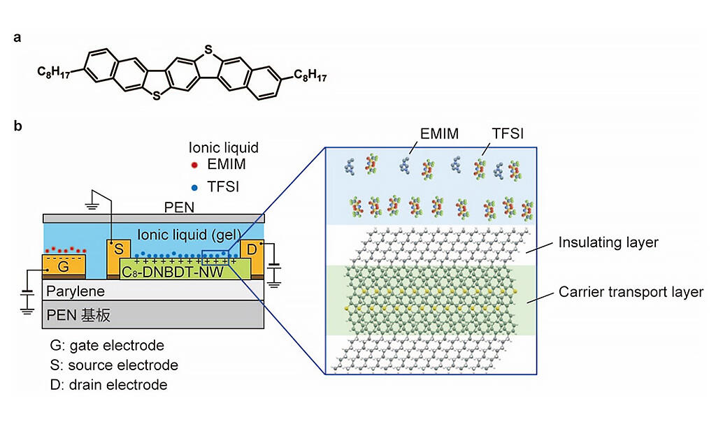
The research group has developed a method and technology for fabricating organic semiconductor single crystal thin films with a thickness of several molecular layers using a printing process. As the surface of the organic semiconductor C8-DNBDT thin film obtained by this technique does not even have the slightest defect, and the number of molecular layers of the thin film can also be precisely controlled, this is an ideal thin film for demonstrating the insulator-metal transition. The group then fabricated an electric double layer transistor structure (EDLT) using this high-quality thin film surface.
In the EDLT, the insulator layer of the common field-effect transistor is replaced with an ionic liquid, and a high-density charge can be injected at small voltages. In this case, when a high density of electron-holes, corresponding to one electric charge per four molecules, was induced in C8-DNBDT using EDLT, a low sheet resistance of approximately 17 kΩ was obtained at 260 K. This value is approximately one order of magnitude lower than when using a general field effect transistor and is sufficiently small compared to the quantization resistance (25.8 kΩ), which is an indicator of insulator-metal transition. By implementing high-density carrier injection, the sheet resistance of the C8-DNBDT thin film continued to decrease monotonously until 10 K, showing a temperature dependency peculiar to metallic states. It was clarified for the first time that a metallic state can be realized even in organic semiconductor crystals.
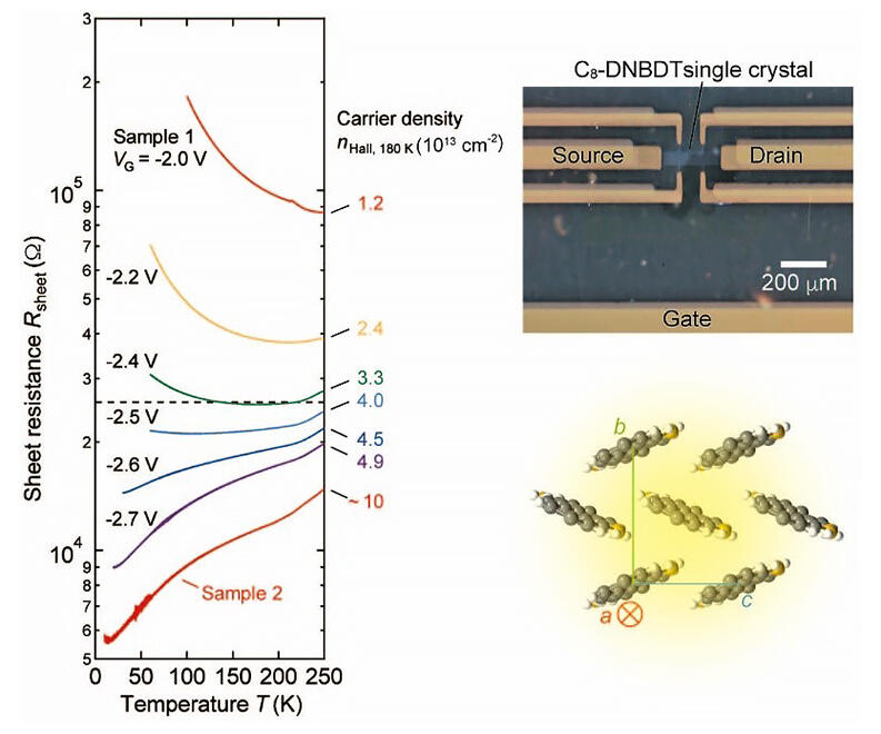
It was also found that the temperature dependence of the carrier mobility obtained by the Hall effect measurement agreed with the standard model of the two-dimensional electron system. Furthermore, it was clarified that a two-dimensional hole gas, in which the charge was confined to one molecular layer, was formed in this system. Two‐dimensional electron gas and two‐dimensional hole gas are generally realized at the interfaces of inorganic materials with precisely controlled atomic layers. In contrast, the formation of the organic two-dimensional hole gas obtained this time was demonstrated on the surface of an organic semiconductor that spontaneously forms an aggregate. The electrical resistance of the organic two-dimensional hole gas was also found to be comparable to that of inorganic materials.
This article has been translated by JST with permission from The Science News Ltd.(https://sci-news.co.jp/). Unauthorized reproduction of the article and photographs is prohibited.