
Associate Professor Norihiro Shimoi, Graduate School of Environmental Studies, Tohoku University (currently, Professor of the Department of Electrical and Electronic Engineering, Tohoku Institute of Technology), and Professor Shun-Ichiro Tanaka, Tohoku University, succeeded to obtain a large-area and uniform morphology ZnO thin film with irradiating wet-process zinc oxide (ZnO) particles with monochrome electron beams from a planar field emission (FE) source using highly crystalline single-walled carbon nanotubes (hc-SWCNTs). This film formed without a heating process exhibited the best reported electrical and optical characteristics.
As the electrical characteristics of ZnO thin films are highly dependent on the crystal growth atmosphere and temperature, the films have not yet to develop high-performance characteristics that can handle mega-data processing required by the IoT evolution of flexible devices.
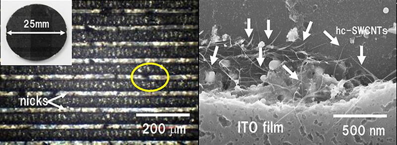
The research group focused on the non-equilibrium reaction field by electron beam irradiation as the bottom-up architecture, which enables construction of local particle binding and unique nanostructures that are unlikely to occur in normal heating processes. They developed a planar electron emission source using hc-SWCNTs as field emitters, and they established a technique to cross-link the nanosized zinc oxide fine particles in two-dimensional shapes.
This is the first reported success in forming a ZnO thin film with high transparency and high conductivity without a heating process on a flexible low-melting-point substrate, for example, polyethylene terephthalate (PET) resin.
It was also found that for improving the transparency and electrical characteristics of ZnO film, it was effective to suppress the scattering at the grain boundaries by aligning the c-axis and reducing the ionization impurity scattering.
Furthermore, they found that the c-axis of each ZnO grain in the particle was aligned with high energy resolution and high acceleration energy of about 90-120 keV. Consequently, they achieved a high transparency of 78% at a wavelength of 550 nm and a high translucency of 90% compared with PET resins.
In addition, the ZnO thin films obtained in this study successfully possess high functional thin films with high electrical properties, including maximum carrier density of 1.8×10¹⁸ per cubic centimeter, hole mobility of 158.6 square cm/Vs, and electrical resistance of 8.6×10⁻⁴ Ωcm, despite being on PET film substrates.
Associate Professor Shimoi said, "Flexible device packaging for constructing highly functional transparent conductive films and thin-film semiconductor devices on resin films will become possible just by using wet processes such as roll-to-roll. We expect that IoT technology will become more and more prevalent in our lives."
This accomplishment may make a significant contribution to the analysis of the formation mechanism of ZnO particles with a uniform morphology and crystal structure by FE electron beam during the crystallization. Moreover, they will be able to provide basic elements for next-generation nanodevices with highly functional properties by controlling each terminal crystal interface of metals, ceramics, and semiconductors with this technique.
■ Non-equilibrium reaction field - When a material is irradiated with an electron beam or ions of several hundred keV, a non-equilibrium reaction is initiated, which is unlikely to occur with normal heating processes.
This article has been translated by JST with permission from The Science News Ltd.(https://sci-news.co.jp/). Unauthorized reproduction of the article and photographs is prohibited.