
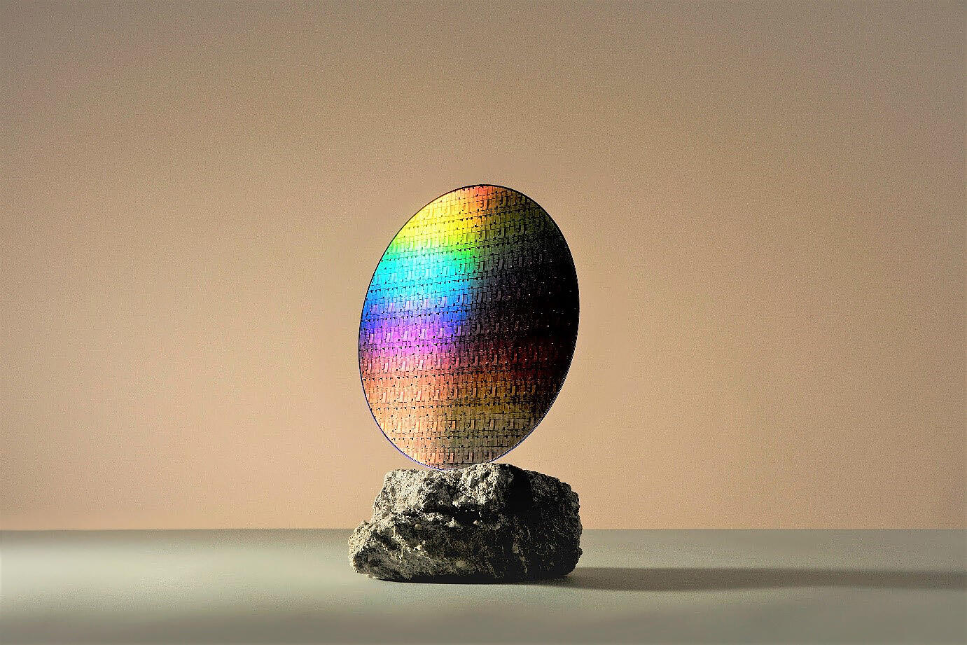
On December 14, IBM and Samsung Electronics jointly announced a breakthrough in semiconductor design by developing a new vertical transistor architecture. This architecture demonstrates a path toward miniaturization beyond nanosheets and has the potential to reduce energy consumption by 85% compared to scaled fin field-effect transistor (finFET). This development was conducted at IBM's semiconductor development base, Albany NanoTech Complex, in New York.
Credit: Connie Zhou for IBM
Moore's Law, which states that the number of transistors mounted on a dense IC doubles every two years, is now rapidly approaching its limits. Due to insufficient space, transistors are packed into a limited area. Conventional transistors have been built such that they lie flat on the surface of a semiconductor and the current flows laterally. However, with the newly developed vertical transport field effect transistor (VTFET), IBM and Samsung Electronics have succeeded in creating transistors that lie perpendicular to the surface of the chip, allowing the vertical flow of current. The forming process of VTFET challenges the limits of Moore's Law, eliminating the various performance barriers that arise as chip designers attempt to pack more transistors into a limited space. Moreover, it is possible to review the connection points of the transistors and allow a larger current flow with reduced loss. The new design aims to enhance the performance and reduce energy-power consumption by 85%, compared to the other technological alternative, the finFET.
This newly developed perpendicular transistor results in breakthroughs such as device architectures that enable semiconductor devices to be scaled beyond nanosheets, cell phone batteries that could go on over a week without being charged, and significant reductions in power consumption and CO2 emissions in processes that require large amounts of power, such as cryptomining and data encryption. In addition, the two companies expect that these breakthroughs will promote the use of low-power devices such as IoTs and edge devices in a wider range of environments, including ocean buoys, autonomous vehicles, and spacecraft.
IBM recently announced a breakthrough in 2-nm chip technology that allows up to 50 billion transistors to be mounted in a fingernail-like space. However, this VTFET innovation focuses on an entirely new dimension that leads to the continuation of Moore's Law. While innovations at the Albany NanoTech Complex are often directly linked to commercialization, the two companies have announced that Samsung Electronics will manufacture the IBM 5 nm node chips at the final stage of the chip development life cycle. These chips are expected to be used on IBM's own server platforms.
This article has been translated by JST with permission from The Science News Ltd.(https://sci-news.co.jp/). Unauthorized reproduction of the article and photographs is prohibited.