
Novel Crystal Technology (Sayama City, Saitama Prefecture), which is working on the development and commercialization of the "β- gallium oxide (Ga2O3) Schottky barrier diode (SBD)"under the "Strategic Energy Conservation Technology Innovation Program"of NEDO (New Energy and Industrial Technology Development Organization), has developed an ampere-class, 1200 V breakdown-voltage gallium oxide Schottky Barrier Diode (SBD). NEDO and the company announced this novel achievement on December 24th. Details of the development were published in the online version of Applied Physics Express and published by the Japan Society of Applied Physics on December 15th.
Through NEDO, the company plans to establish a manufacturing process and ensure the reliability of the 1200 V, pressure-resistant gallium oxide SBD that was successfully prototyped in this project, while also aiming for commercialization in 2023. Simultaneously, the company will construct a 100 mm mass production foundry line for the high-quality, gallium oxide, 100 mm epi wafer that was launched in June last year. Compared to silicon carbide (SiC) and gallium nitride (GaN), which are also being developed as high-performance materials to replace silicon, gallium oxide features excellent material properties and is produced using a low-cost crystal growth method. Hence, it can be used to fabricate low-loss, low-cost power devices.
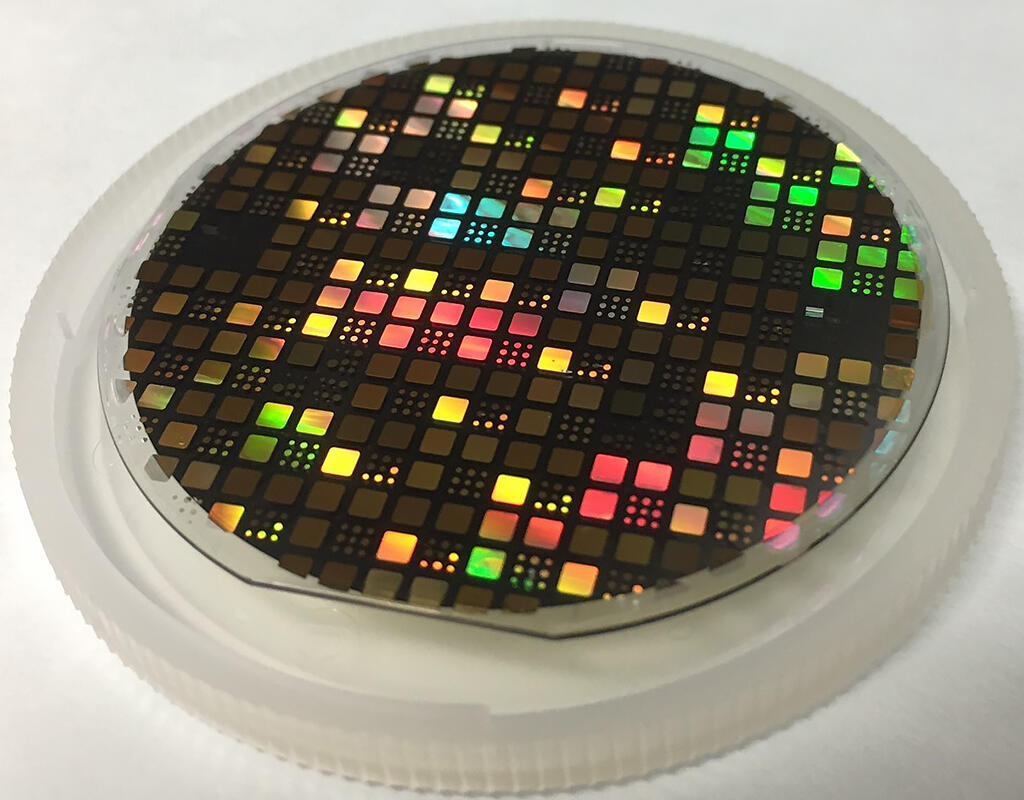
Novel Crystal Technology has been working toward commercializing gallium oxide devices since 2017 and demonstrating the gallium oxide SBD as a part of NEDO's "Strategic Energy Conservation Technology Innovation Program." This time, using a research prototype line and foundry, the company has developed a mass production process for a trench-type gallium oxide SBD on a 2-inch wafer, as well as the world's first ampere-class gallium oxide SBD with a breakdown-voltage of 1200 V. The high-voltage gallium oxide SBDs that will be developed are expected to have applications such as next-generation quick chargers, for which the demand for higher voltages and power is expected to increase in the future.
Prior to this achievement, Tamura Corporation, the parent company of Novel Crystal Technology, succeeded in developing the world's first gallium oxide epi wafer for power devices in 2015, by participating in NEDO's "Energy-saving innovation technology development business / R&D of ultra-high breakdown-voltage gallium oxide power device"project from FY2011 to FY2013. In addition, since FY2018, the company has been promoting the development of gallium oxide SBDs for their practical applications in power devices under NEDO's subsidized project "Strategic Energy Conservation Technology Innovation Program / Development of Ampere-Class Gallium Oxide Power Devices." Conventionally, a planar structure, which is relatively easy to process, has been used for the development of high-current gallium oxide SBDs. However, as planar-type SBDs suffer from high leakage currents, it is difficult to produce a gallium oxide SBD with a withstand voltage of 1200 V.
Meanwhile, in 2017, the company succeeded in demonstrating the principle of trench-type gallium oxide SBDs, which reduces the reverse leakage current by 1/1000th, and has since been improving the device's withstand voltage and current. Furthermore, this time, using the research prototype line and foundry together, the company developed a process for the mass production of 2-inch wafers and succeeded in prototyping an ampere-class, 1200 V withstand voltage, trench-type gallium oxide SBD. This makes it possible to develop a mass production process using the 100 mm foundry line, in order to evaluate the performance and reliability of the 1200 V withstand voltage gallium oxide SBDs at the mounting circuit level, as well as to encourage the commercialization of low-loss gallium oxide power devices. In addition, the market share of medium- and high-voltage high-speed diodes, which is expected to expand to 120 billion yen in 2022 and 150 billion yen in 2030 (Fuji Keizai "2021 version of the next-generation power device & power electronics related equipment market status and future prospects") will benefit from this development, and the company is expected to enter this market with its gallium oxide SBD.
This article has been translated by JST with permission from The Science News Ltd.(https://sci-news.co.jp/). Unauthorized reproduction of the article and photographs is prohibited.