
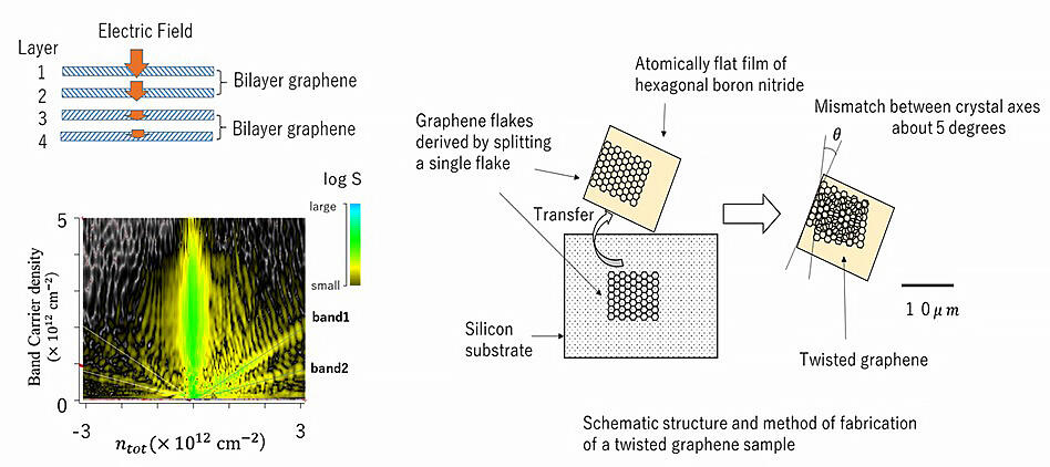
It has been difficult to clearly observe the layer-by-layer screening of electric fields with graphite, which is crystal that forms graphene. Understanding the state of such a screening process is crucial for designing an atomic-layer device and analyzing its electronic state during operation. For the first time, the research group led by Ryuta Yagi, Associate Professor, Graduate School of Advanced Science and Engineering, Hiroshima University, and members of the National Institute for Materials Science, succeeded in microscopically clarifying this problem from the viewpoint of transport phenomena using twisted double bilayer graphene, which is artificially created by stacking bilayer graphene. According to Associate Professor Yagi, "If the form of graphene is different, the electronic structure is completely different. Our research is underway to clarify this, but for some reason, the theoretical calculation and experimental results do not match. We expected this difference to arise from the screening effect of the electric field."
Twisted graphene was fabricated by dividing bilayer graphene obtained by cleaving graphite with adhesive tape into two parts using atomic-layer transfer technology, then artificially stacking the obtained samples, with the crystal angles of each bilayer graphene shifted by approximately 5 °, and finally sandwiching them between atomically flat hexagonal boron nitride thin films. The research group measured the dependence of the electrical resistance on the magnetic field in this twisted double bilayer graphene device. The magnetic quantum oscillations that appear in response to changes in the magnetic field at low temperatures were investigated in detail. The results revealed that the electron densities of the upper and lower layers of the bilayer graphene were not equal; this clarified the state of screening of the electric field at the atomic-layer thickness.
Provided by Hiroshima University
Comparing this result with the results of the same experiments performed thus far on a four-layer but naturally occurring crystal structure (AB lamination), it was found that the screening length of the twisted double bilayer graphene may be longer. These differences suggested that the quantum mechanical wavefunction extending in the layer direction is limited to each bilayer in the twisted double bilayer graphene, but is generated from the difference arising due to it being spread over four layers for the AB-laminated graphene. This result was published in the December issue of JPSJ.
Associate Professor Yagi concluded, "Spintronics using electrons is a vast field, but we are contemplating the use of the valley structure that appears in the electronic structure to create an element with a new operating principle that can replace spintronics. In the future, it is expected to lead to the development of electronic products that do not contain harmful substances, as well as to the development of light and flexible home appliances. In addition, it is possible that this could be expanded to communication equipment, solar cells, interfaces between nerves and electronic devices, and so on."
This article has been translated by JST with permission from The Science News Ltd.(https://sci-news.co.jp/). Unauthorized reproduction of the article and photographs is prohibited.