
In the "Strategic Innovation Program for Energy Conservation Technologies" of NEDO (The New Energy and Industrial Technology Development Organization), Asahi Denka Kenkyusho Co., Ltd., ALPHASEIKO Co., Ltd., and Synapse LLC have succeeded in developing electronic components (width of 1.2 mm and thickness of 0.25 mm) that are thinner and smaller and exhibit superior transmission properties compared with those of the conventional ones using MEMS technology (Micro Electro-Mechanical Systems). Conventional MEMS technology uses only silicon and is limited to sensors; however, the newly developed technique uses metals and resins, making it applicable to a wide range of electronic components such as connectors, sockets, switches, and inductors, as it uses metals and resins. NEDO intends to apply this effective result to fine, high-performance electronic components used in smartphones and other devices and contribute to the evolution of 6G and energy-saving.
With the initiation of the commercial services of 5G (fifth-generation mobile communication system), post-5G and -6G technological developments with enhanced functions, such as ultra-low delay and multiple simultaneous connections, are progressing in Japan and other countries. Electrical connectors and semiconductor sockets used in such next-generation communication need to be thinner and miniaturized and should exhibit excellent high-frequency transmission characteristics. However, in the conventional insert molding technique, which integrates metal and resin by injecting resin around metal parts inserted into the mold (the mold press method), as warping occurs, it is difficult to mold small, thin components of a thickness of ~0.8 mm or less. Furthermore, as the connection length is long, it was not possible for components that satisfy the required transmission characteristics to be realized.
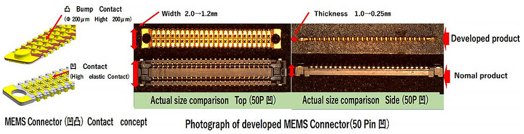
This time, as part of the "Strategic Energy Conservation Technological Innovation Program", NEDO and three companies in collaboration with the Tokyo Institute of Technology and National Institute of Advanced Industrial Science and Technology, developed a new manufacturing method in which concave-convex terminals are added and molded on copper-clad films as base metals using the MEMS technique. "Micro-electro-mechanical systems (MEMS)" are devices with a micron-level structure in which mechanical components, such as sensors, actuators, and electronic circuits, are integrated into a semiconductor-based silicon substrate. Using the proposed MEMS-based technique, a connector that is 2.0 mm wide and 1.0 mm thick has been miniaturized into a thinner one with a width of 1.2 mm and a thickness of 0.25 mm. Using the proposed method, the size of components, which are extremely thin (0.1-0.5 mm), can be reduced to less than one third of the conventional ones. Therefore, the length of the terminal connection part can be shortened, the electrical inductance can be reduced, and the transmission characteristics can be improved.
Thus, in the high-frequency transmission band of 1-30 GHz to be used in the 6G generation, which is currently being developed, it satisfies the transmission characteristics, that is, the insertion loss to be approximately -3 dB and the mismatch of the characteristic impedance to be 5 Ω or less, and enables the production of electronic components that achieve significant energy-saving. Conventional MEMS techniques can only use silicon, and application is limited to sensors and related components. As the proposed technique uses metals and resins, it can be applied to various electronic components, e.g., connectors, sockets, switches, inductors, heat sinks, semiconductor packages, ultra-fine FPCs, and micromotor components.
Using the proposed method, the group has succeeded in developing a MEMS connector that is 1/4 the thickness and less than 1/6 the weight of the conventional connector, considering the two-row-type connectors used in smartphones, notebook PCs, gaming machines, and other devices. The transmission loss is approximately one fourth of that of the conventional product, and the amount of metal and resin used is remarkably reduced, making it an energy- and resource-saving product from the viewpoint of materials. When this connector is used in smartphones and other devices, energy consumption can be reduced by 55% compared to the conventional one.
The group has also succeeded in developing semiconductor sockets, which connect components for testing and mounting memories and logic-based semiconductors. Most logic-based semiconductor packages mounted on smartphones or PCs have a large number of solder balls on the mounting surface. As there is an increase in the miniaturization of semiconductors, the number of solder balls is increasing every year, and the ball pitch is becoming smaller, making it difficult and expensive to manufacture semiconductor sockets for testing them. The group developed thin semiconductor sockets that can be tested and mounted on a logic-based ball grid array (BGA)-type semiconductor package with 1500-2500 pins and a pin pitch of 0.3-0.5 mm. Moreover, this socket can accommodate solder balls with pitch reduced to 0.3 mm. Until now, testing could only be performed using an expensive socket in which long probe pins (for connection) with built-in coil springs are arranged in a grid pattern; however, recently, by fabricating contact devices in batches using MEMS, the group has realized a socket that can handle high frequencies and save energy, thereby reducing its cost.
In the future, after the completion of NEDO's Strategic Energy Conservation Technological Innovation Program, the three companies will continue to work on mass production, low-cost processing technology, yield improvement, and further development of high-precision processing technology. They will apply the aforementioned technologies to micro and high-performance electronic components used in smartphones and other devices, aiming to evolve into 6G communications systems and save energy.
This article has been translated by JST with permission from The Science News Ltd.(https://sci-news.co.jp/). Unauthorized reproduction of the article and photographs is prohibited.