
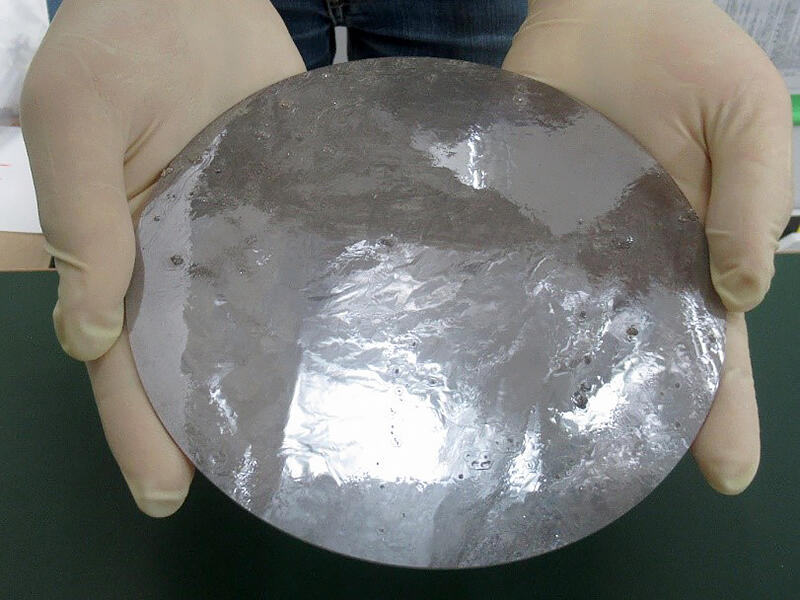
A research group led by Associate Professor Masayuki Imanishi and Professor Yuusuke Mori of the Graduate School of Engineering at Osaka University, in collaboration with Panasonic Holdings, Toyoda Gosei and SCIOCS, has successfully grown the world's largest 6-inch, high-quality GaN (gallium nitride) crystals with the sodium flux method under a project implemented by the Ministry of the Environment. They also demonstrated for the first time in the world that the use of GaN crystals can improve the device characteristics of high performance vertical GaN transistors.
Courtesy of Osaka University
Courtesy of Osaka University
The research group has developed a completely new technique for growing GaN crystals with the sodium flux method using a multipoint seed with many micro seed crystals on a sapphire substrate. With this technology, GaN crystals naturally separate from the sapphire substrate when brought back to room temperature after growth, making it possible to grow large GaN crystals with extremely low warpage. Using this technology, they were able to fabricate high-quality 6-inch, large-diameter GaN crystals with minimal warpage for the first time in the world.
Furthermore, the research group demonstrated for the first time that the device characteristics of vertical GaN transistors can be improved by using GaN crystals fabricated with the sodium flux method. Even with GaN crystals fabricated by the conventional HVPE method, it has been possible to obtain significant high-performance vertical GaN transistor characteristics through creative structure design. However, when fabricating more complex vertical GaN transistors, there are serious practical problems, such as the fact that only three of the 10 transistors fabricated will operate properly. The cause of this problem has not been identified.
However, using GaN crystals fabricated with the sodium flux method solved this problem. Specifically, the GaN crystals fabricated by the research group dramatically improved the transistor yield to 72%, compared to 33% for commercially available conventional GaN crystals.
"We can mass produce high-quality, large-diameter GaN wafers at low cost by using GaN crystals fabricated with the new method as seed crystals and growing them in bulk by other methods (HVPE method, ammonothermal method, OVPE method) to fabricate GaN wafers," explains Professor Mori. "We hope that these GaN wafers will enable the fabrication of devices that could not be realized before, such as high-performance power devices and radars, thereby contributing to energy conservation and 5G/6G."
■ Sodium Flux Method: A method of depositing GaN crystals by mixing sodium (Na) and gallium (Ga) and exposing them to high-pressure nitrogen at 850°C and about 40 atmospheres of pressure.
This article has been translated by JST with permission from The Science News Ltd.(https://sci-news.co.jp/). Unauthorized reproduction of the article and photographs is prohibited.