
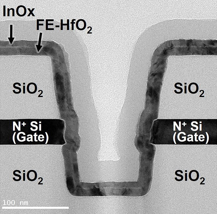
A joint research group led by Associate Professor Masaharu Kobayashi of Institute of Industrial Science (IIS), the University of Tokyo and Professor Yukiharu Uraoka of Nara Institute of Science and Technology (NAIST) has developed a technology for depositing the semiconductor oxide indium oxide (In2O3) using atomic layer deposition (ALD) instead of the typical sputtering method, and developed a 3D vertically formed ferroelectric and antiferroelectric transistor memory.
(Provided by Professor Masaharu Kobayashi, Institute of Industrial Science, the University of Tokyo)
As the use of Big Data continues to advance, high-capacity, low-power consumption storage memory will be required not only in cloud servers but also in IoT edge devices. The research group focused on ferroelectric field-effect transistors (FeFET) to produce memory cells and developed a three-dimensional stacked-channel FeFET by depositing oxide semiconductors, which are typically deposited by sputtering, using the atomic layer deposition method. They also developed an antiferroelectric field-effect transistor (AFeFET) memory cell that can be rewritten more efficiently.
Thin-film transistors fabricated using In2O3 deposited by ALD showed high mobility of >40Vs per square centimeter. They succeeded in using the ALD method to deposit In2O3 uniformly in a 3D structure. Using this deposition technique, the research group made a prototype FeFET with a gate dielectric of hafnium zirconium dioxide (HfZrO2), which can also be deposited by ALD, and as theoretically predicted, demonstrated a memory window (threshold voltage difference) of about 1.5 V, a write endurance exceeding 104 times, and retention properties exceeding 103 seconds.
Furthermore, they proposed an antiferroelectric transistor (AFeFET) using antiferroelectric ZrO2 as the gate dielectric. Oxide semiconductors are N-type semiconductors, and while they easily induce electrons, which are the majority carriers, they have difficulty traversing holes, which are minority carriers, and thus have the characteristic of degrading the retention characteristics of the erase state relative to the program state. The use of an antiferroelectric allows for an efficient erase operation without inducing minority carriers and improves the retention characteristics of the erase state. In fact, the research group was able to demonstrate a memory window of about 0.7 V, a write endurance of over 104 times, and a retention characteristic of over 103 seconds.
"Since this memory device technology has high density and low power consumption, it shows promise for use for storage memory in IoT devices to develop social services that make use of Big Data," explains Associate Professor Kobayashi. "We will continue to develop device design, materials, and processes to achieve higher integration and reliability, and aim to incorporate high-capacity storage memory in IoT edge devices."
■ Atomic layer deposition (ALD) method: A conventional method of chemical vapor deposition. A reaction precursor is supplied to a chamber in a pulsed manner for a short time to saturate a monolayer of molecules on a wafer to be deposited, and then water or oxygen, which serves as an oxidant, is supplied in a pulsed manner for a short time to oxidize the saturated molecular layer to form atomic layer oxides. By repeating this process, a film can be formed for each atomic layer. The feature of this method is that it is capable of uniform film deposition with little loading effect, not only on flat surfaces, but also on 3D structures.
This article has been translated by JST with permission from The Science News Ltd.(https://sci-news.co.jp/). Unauthorized reproduction of the article and photographs is prohibited.