
On June 29, a research team led by senior researcher Guangwei Cong of the National Institute of Advanced Industrial Science and Technology (AIST)'s Platform Photonics Research Center, announced the development of an ultra-low latency, low power consumption neural network computing technology using silicon photonic circuits instead of electronic circuits. The technology was developed jointly with NTT. The results were published in Nature Communications, a Springer Nature publication, on June 30. The project was funded by the Japan Science and Technology Agency's CREST program.
The newly developed technology uses silicon photonic circuits to perform machine learning calculations. Silicon photonic circuits are high-density integrated optical circuits based on silicon optical waveguides produced on silicon wafers.
The electrical signals from the multidimensional data being analyzed are input to the different input ports of this photonic circuit and converted into optical signals. Calculations are performed as the signal passes through several optical interferometers incorporated in the photonic circuit. The result of the calculation is output as the light intensity distribution of multiple output ports.
Using this technology, the team was able to perform neural network operations using photonic circuits alone (without incorporating electrical circuits). The calculation is completed simply by propagating light through a photonic circuit with fixed parameters.
This method means that sequential switching, as in digital electronic circuits, is no longer necessary. Operations can, therefore, be performed with a delay time of less than 1/1000 of an electronic circuit and power consumption of several 10ths that of an electronic circuit. Photonic circuits can also apply a high-speed clock 10 times faster than electronic circuits, allowing for more data processing per unit of time.
In the study, a nonlinear mapping neural net calculation scheme was proposed to use the nonlinearity of optical interferometer devices with respect to the driving voltage. This calculation method sees the data to be analyzed being mapped nonlinearly to a high dimensional optical complex amplitude space through an optical interferometer device in the data input section. The calculation results are obtained by optical propagation to a photonic circuit consisting of several optical interferometers.
To verify this calculation method, the team fabricated the photonic circuit using silicon photonic technology. It then attempted to perform classification calculations on this circuit using a benchmark called Iris classification, which determines the variety of an iris based on the size of its petals.
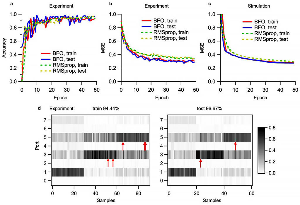
Cong, G., Yamamoto, N., Inoue, T. et al. On-chip bacterial foraging training in silicon photonic circuits for projection-enabled nonlinear classification. Nat Commun 13, 3261 (2022).
https://doi.org/10.1038/s41467-022-30906-3 (CC by 4.0)
The classification is correct if the ports outputting the maximum optical power match the ports assigned to each iris species. Before learning was performed, the classification could not be performed. However, after learning from 90 samples, the method enabled correct classification approximately 94% of the time. Classification was also performed on 60 unlearned samples, yielding a correct response rate of approximately 97%.
The processing time for the classification (the time it takes for light to pass through the photonic circuit) was less than 100 picoseconds, about 1/1000 of a calculation using a digital electronic circuit. The heater power required to set the circuit parameters was about 360 milliwatts, several 10ths of that required for digital electronic circuits.
If the interferometers for data input were changed from heater types with slow responses to high-speed silicon modulators with PN junctions that can operate at 10s of GHz, the team expects that, in principle, high throughput of 10s of billions of calculations per second will be possible.
Based on these characteristics, AIST and others expect that this neural network computation technology, which operates only with silicon photonic circuits, can be applied to AI accelerators that complement digital electronic circuits. AI accelerators are arithmetic circuits specialized for high-speed AI processing. However, conventional optical neural network arithmetic circuits use a hybrid configuration in which optical signals are converted to electrical signals, and digital calculations are performed by electronic circuits due to the difficulty of integrating nonlinear response devices that use light. This limitation means that the benefits of optical neural network operations, such as power consumption and calculation latency, have not yet been utilized. Researchers have therefore been hoping for a technology that enables neural network operations using only photonic circuits.
This article has been translated by JST with permission from The Science News Ltd.(https://sci-news.co.jp/). Unauthorized reproduction of the article and photographs is prohibited.