
A joint research team consisting of graduate student Ryoki Hashimoto, Assistant Professor Hiroo Suzuki, Assistant Professor Masaaki Misawa, Professor Kenji Tsuruta and Professor Yasuhiko Hayashi, all of the Graduate School of Natural Science and Technology, Okayama University, in conjunction with Associate Professor Yasumitsu Miyata of the Department of Physics, Graduate School of Science, Tokyo Metropolitan University, has succeeded in the large-area, high-quality synthesis of transition metal dichalcogenides (TMDCs), which are semiconductor materials with atomic-level thinness, with a new chemical vapor deposition (CVD) method using a confined space.
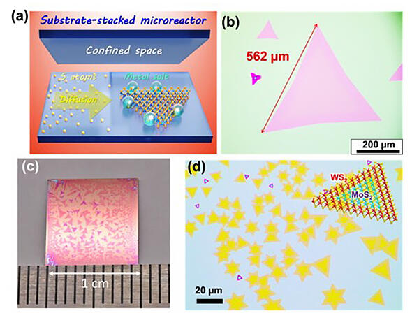
(b) Optical micrograph of the large monolayer WS2 crystal.
(c) Optical micrograph of the wafer on which huge WS2 has grown.
(d) Optical micrograph of the lateral WS2/MoS2 heterostructures. The inset shows the schematic of the lateral WS2/MoS2 heterostructure.
Provided by Yasuhiko Hayashi and Hiroo Suzuki at Faculty of Natural Science and Technology, Okayama University
TMDCs are a layered semiconductor material whose monolayer is a mere three atoms thick and are known as direct band gap semiconductors that have luminescence properties only in a single layer. In addition, these monolayer TMDCs have excellent mechanical flexibility, optical properties and electrical properties, which makes them promising for use in next-generation optoelectronic devices. However, in the conventional CVD method using solid raw materials, the crystal size of the obtained TMDCs is small and the crystallinity is low, which is thought to be a factor in degrading device performance, so there has been a demand to develop a technique for synthesizing large-size TMDC crystals with high crystallinity.
Therefore, the research team set out to produce large-size, high-quality synthesis with tungsten disulfide (WS2), a type of TMDC. To achieve a stable TMDC growth environment, the team constructed a microreactor by overlapping two synthetic substrates to create a narrow, confined space and a growth environment in which the supply of raw materials from the outside is limited. Also, as a raw material for tungsten, a metal salt (Na2WO4) that becomes liquid at high temperatures was applied to the growth substrate in advance, confining it inside the microreactor. For the raw material for sulfur used in WS2, the team employed organic sulfur, for which the amount supplied can be better controlled than conventional solid raw materials, which allowed the team to control the synthesis of monolayer WS2 with high precision.
When the research team precisely controlled the balance of raw materials supplied, they obtained large fully monolayer WS crystals of over 500 μm, whereas crystals of only a few tens of micrometers could be obtained with the conventional CVD method. They also obtained giant crystals that exceeded 1 mm in size and were visible to the naked eye by adjusting the conditions. Furthermore, the combination of two metal salts (Na2WO4 and Na4MoO4) has enabled the synthesis of in-plane heterostructures in which two types of TMDCs (WS2 and MoS2) are joined in the plane.
When the team studied the growth mechanism of WS2, they found from the variation of crystal size with synthesis temperature, fractal growth of a peculiar crystal growth style, and from the theoretical calculation of the surface diffusion energy of the material, they found that the diffusion of the material in the microreactor is the rate-limiting process, and that the growth is controlled by the surface diffusion. Focusing on the luminescence (photoluminescence: PL) properties of WS2 synthesized at different temperatures, they examined the crystal quality and found that in TMDCs with low crystallinity, the PL peak shifted toward lower energy (longer wavelength), the half-width became larger, and the luminescence intensity was weaker. A systematic examination of the PL properties and their uniformity with respect to synthesis temperature confirmed that the optimal synthesis temperature (820°C) produced PL properties that were uniform in-plane and of high quality, while a temperature that was too high or too low resulted in poor crystal quality and uniformity.
"We believe that nanoscale material synthesis using confined spaces offers many degrees of freedom," says Assistant Professor Suzuki. "We would like to challenge new material synthesis with unique ideas, such as confining multiple raw materials together or combining various synthetic substrates. We will also expand into new technologies that allow us to control the properties of materials through the design of the growth space."
This article has been translated by JST with permission from The Science News Ltd.(https://sci-news.co.jp/). Unauthorized reproduction of the article and photographs is prohibited.