
OKI Electric Industry Co., Ltd. (OKI) and KRYSTAL, Inc. announced that they have established a bonding technology for piezoelectric single-crystal thin films and SOI wafers, and have succeeded in producing prototype piezoelectric single-crystal thin-film bonded wafers, which dramatically improve the performance of piezoelectric MEMS devices, such as ultrasonic sensors. The prototype MEMS ultrasonic sensor fabricated using this bonded wafer achieved a sensor sensitivity (transmitting/receiving power efficiency) more than 20 times higher than that of conventional polycrystalline thin films. The two companies will begin shipping samples targeting piezoelectric MEMS device manufacturers by November and aim to provide custom wafers to meet various requirements by 2023.
Provided by OKI
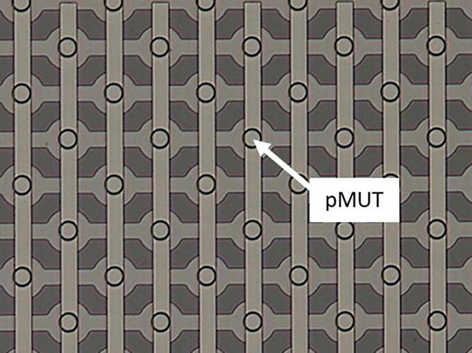
Piezoelectric MEMS devices are used in ultrasonic sensors for object detection, compact microphones and speakers, and high-frequency filters for communication applications. Demand is growing in many market sectors, including automobiles, robots, wearable devices, IoT, smartphones, and communication base stations.
However, these applications demand further miniaturization and lower power consumption, and improving basic characteristics at the material level has proved to be a challenge. Piezoelectric thin films, which determine the basic properties of piezoelectric MEMS devices, are known to have improved properties owing to their single crystallization.
However, forming single-crystal thin films on wafers requires a special buffer layer, limiting the feasible device structures. For this reason, polycrystalline thin films have generally been used. They have inferior properties but are easier to manufacture.
OKI and KRYSTAL have established a technology for direct bonding to SOI wafers using OKI's proprietary CFB technology, which joins substrates made of different materials by intermolecular force without using an adhesive, to strip only KRYSTAL's high-performance PZT (lead zirconate titanate) piezoelectric single crystal thin film from the buffer layer. The prototype piezoelectric single-crystal thin-film bonded wafers fabricated with this technology can be used in various device structures because only the single-crystal thin-film can be directly mounted on the device without a buffer layer. Furthermore, measurements of a prototype MEMS ultrasonic sensor fabricated using this bonded wafer showed that the sensitivity of the ultrasonic sensor was improved by more than 20 times (product of four times transmission and six times reception) compared to conventional polycrystalline thin films.
The results demonstrate that the bonding technique does not compromise the high performance of the piezoelectric single-crystal thin films and that the bonded wafers can be applied to the existing MEMS process device manufacturers.
This article has been translated by JST with permission from The Science News Ltd.(https://sci-news.co.jp/). Unauthorized reproduction of the article and photographs is prohibited.