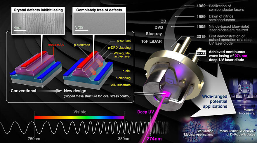
A research group led by Professor Hiroshi Amano, Designated Professor Chiaki Sasaoka, and Lecturer Maki Kushimoto at the Institute of Materials and Systems for Sustainability, Nagoya University, in collaboration with Asahi Kasei Corporation, has successfully demonstrated the world's first room temperature continuous operation of a 274 nm deep UV semiconductor laser (UV-C LD) in the UV-C region. "It has been said that deep ultraviolet was impossible because of how hard it is to make a semiconductor laser as the wavelength becomes shorter," commented Amano. In 2017, Nagoya University and Asahi Kasei launched a joint project, which succeeded in pulsed lasing after two years and led to continuous-wave lasing at room temperature after five years. My own experience with blue lasers took 11 years. There were many factors, including the support of people with experience in LED development and Asahi Kasei, and the dedicated clean room at Nagoya University, but the fact that our wonderful young researchers got into the research and did it so well led to our success in a short period of time." The group's research was published in Applied Physics Letters and in the Nagoya University Repository.

Image credit Issey Takahashi, provided by Nagoya University
There is anticipation that deep-ultraviolet semiconductor lasers can be used in various fields such as healthcare, measurement and analysis, sensing, and laser processing, including high-speed and large-area sterilization, Raman spectroscopy, molecular detection using resonant plasmon, and microlithography.
In 2019, the joint research group succeeded in lasing a deep-ultraviolet semiconductor laser in the UV-C region at room temperature with a pulsed current drive for the first time in the world. However, because of the high threshold current, pulse lasing at the time required as much as five watts of power, and continuous-wave lasing was difficult due to the heat generated.
The group focused on the crystal defects that occur at the edge of the mesa stripe (a rectangular shape carved into the semiconductor multilayer film structure, including the active layer that generates the ultraviolet light, with the long side in the direction of light propagation). Crystal defects not only worsen the threshold current density, but also worsen the current flow by putting restrictions on electrode design.
Kushimoto explained, "When we looked at the crystal defects in the mesa stripes with an electron microscope, we found that multiple defects existed in a continuous longitudinal direction, so we thought that this might be caused by some kind of force." Through repeated simulations, prototyping and modelling, we found that the structural stresses in the mesa stripe were caused by defects."
The research group then devised a device structure to minimize the stress. Specifically, when viewed from the side, instead of the conventional square structure, the wall near the light emitting part is tilted from 90° degrees to 15° to alleviate the concentration of force. As a result, they were able to create a device with no defects at all at the edge of the mesa stripe. At the same time, by improving the conditions for thin-film crystal growth, they lowered the threshold current to about a quarter of that of the conventional structure to achieve a threshold current density of 4.2 kA/cm2.
The resistance of the electrodes was as high as 15.9 Ω because the conventional structure avoided the crystal defects at the edge of the mesa stripe, but the elimination of crystal defects enabled the electrodes to be placed close to the edge stripe, which significantly reduced the resistance to 8.3 Ω, the highest level in the world.
The result of these improvements was a deep-ultraviolet semiconductor laser that can be powered by a 9 V dry cell battery at 8.7 V and 0.125 A. "In our research, the output power is at the 2-mW level, which is about the same as a laser pointer, but we would like to increase the output power to the watt level in the future," Amano said.
"We hope to ship samples from Nagoya University in 2025 and commercialize the technology at Asahi Kasei in 2026," added Naohiro Kuze, an executive officer at Asahi Kasei. "Since most of the equipment for the LED project is available, we believe that the necessary equipment can be installed in about one year. First, we are considering commercializing it in the field of measurement and analysis. By increasing the output [of the laser], the areas for commercialization will expand. Moving forward, we would like to aim for a watt class and consider expanding into the processing field."
Journal Information
Publication: Applied Physics Letters
Title: Key temperature-dependent characteristics of AlGaN-based UV-C laser diode and demonstration of room-temperature continuous-wave lasing
DOI: 10.1063/5.0124480
Journal Information
Publication: Applied Physics Letters
Title: Local stress control to suppress dislocation generation for pseudomorphically grown AlGaN UV-C laser diodes
DOI: 10.1063/5.0124512
This article has been translated by JST with permission from The Science News Ltd. (https://sci-news.co.jp/). Unauthorized reproduction of the article and photographs is prohibited.


