
The miniaturization of semiconductors has been ongoing over the years to the point where today's devices contain billions of transistors. However, for further miniaturization to occur, the increase in defects associated with miniaturization must be controlled. This is because defects increase power consumption and lead to malfunctions. However, it is necessary to understand the mechanism of the oxidation reaction at the atomic level of film thickness in order to precisely control the oxidation reaction and fabricate high-quality oxide films with few defects on silicon substrates.
A research group led by Yasutaka Tsuda and Akitaka Yoshigoe of the Materials Sciences Research Center, Japan Atomic Energy Agency (JAEA), Professor Yuji Takakuwa and Assistant Professor Shuichi Ogawa of Tohoku University, and Professor Yukio Yamamoto of the National Institute of Technology, Fukui College (KOSEN), has identified the growth mechanism of silicon oxide films through real-time photoemission spectroscopy observations using high-brilliance synchrotron radiation at SPring-8. "We used parameters like temperature conditions, pressure and oxygen speed," explained Tsuda. "When we didn't know the mechanisms, we manipulated them by brute force to find the conditions. Now that we have an understanding of these, we will be able to establish guidelines as to which process is best for the creation of a state with fewer defects." The researchers' findings have been published online in the Journal of Chemical Physics.
Provided by JAEA
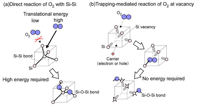
The growth of an oxide film on a silicon substrate, for example SiO2, is a reaction at the SiO2/Si interface with O2 being absorbed from the surface of the oxide film and diffusing inward. It was thought that the reaction of O2 at the SiO2/Si interface occurs in an order of direct reaction of the Si-Si bond with O2 to form a Si-O-Si bond. However, for such a reaction to occur, O2 must have a high kinetic energy. This explanation is contradictory because the average kinetic energy of the O2 molecules is low for oxidation by O2 gas.
In this research, the group focused on defects at the SiO2/Si interface. The SiO2/Si interface is subject to large strain due to the volume expansion associated with SiO2 formation. This strain is known to be the cause of the formation of defects at the interface. The research group had previously found that O2 reacts at these defects. However, they had no idea how this reaction was occurring.
They surmised that carriers (electrons and holes that contribute to electrical conduction in semiconductors) would become chemically reactive by associating with defects and reacting with O2 and demonstrated this with real-time photoemission spectroscopy using synchrotron radiation. They also found that O2 is adsorbed as a molecule in the resulting reactive defects. The O2 then dissociates into oxygen atoms, forming a Si-O-Si bond. No energy is required for such a molecular adsorption reaction pathway. In other words, there are no conventional contradictions, and the experimental results can be explained in a natural way.
The researchers proposed a new reaction mechanism in which the reaction of O2 at the SiO2/Si interface proceeds by a process of molecular adsorption on defects and that the carriers of the Si substrate are involved in the reaction process.
This oxidation model can be applied in various ways. For example, it can be used to explain why the previously unknown oxidation rate is different between p-type Si and n-type Si. Their findings will lead to the establishment of fundamental technologies that are essential to the design and manufacturing process of CMOS, which will continue to play an important role in the future. The fact that O2 reacts with defects also suggests that SiO2 growth is possible while eliminating defects.
This article has been translated by JST with permission from The Science News Ltd. (https://sci-news.co.jp/). Unauthorized reproduction of the article and photographs is prohibited.