
On April 10, 2023, NEC announced that it had successfully developed the world's first high‐sensitivity uncooled infrared image sensor using high‐purity semiconducting carbon nanotubes (CNTs) for the infrared detection area based on its proprietary extraction technology. The company aims to commercialize this image sensor by 2025.
Provided by NEC
An infrared image sensor converts infrared radiation into an electrical signal to acquire necessary information. It can detect infrared radiation emitted from humans and objects in the dark and is employed in various fields, such as in night vision systems to support automobile driving at night, navigation support systems for aircraft and security cameras, to realize safe and secure social infrastructure.
Two types of infrared image sensors have been developed to date: a 'cooled type' that must be cooled to a very low temperature for operation and an 'uncooled type' that operates near room temperature. While the 'cooled type' is highly sensitive and responsive, it presents certain drawbacks such as the requirement of large and expensive cooling systems, high electricity consumption and periodic maintenance needs.
By contrast, the 'uncooled type' is small, inexpensive, and consumes low power because it does not require a cooling system. However, compared with the 'cooled type,' the 'uncooled type' presents an inferior sensitivity and resolution.
Against this background, NEC has focused on semiconductor‐type CNTs, contained within single‐walled CNTs, with temperature‐sensitive resistance values. The company has now succeeded in developing the first high‐sensitivity uncooled infrared image sensor using a semiconductor‐type CNT film for the infrared detection area.
CNTs are carbon materials discovered in 1991 by Sumio Iijima, the company's Senior Research Fellow. Similar to graphite, CNTs have a cylindrical structure composed of a hexagonal carbon network. This single‐layer cylindrical structure is referred to as a single‐walled CNT, which exhibits either semiconducting or metallic properties depending on the arrangement of the hexagons. When produced, CNTs contain semiconducting and metallic components at a ratio of 2:1. Since this discovery, the company has been conducting research and development, leading to advances in nanotechnology.
In 2018, they developed a unique technology to explicitly extract the semiconducting component with high purity from a single‐walled CNT containing a mixture of metallic and semiconducting components immediately after synthesis. At around room temperature, a thin film of semiconducting CNTs extracted using this technology was found to demonstrate a large temperature coefficient of resistance (TCR: the rate of change in resistance per 1 K between certain temperatures).
This infrared image sensor was developed based on these achievements and knowledge. The sensor utilizes semiconductor‐type CNTs based on a proprietary technology, achieving a high TCR, which is an important index for high sensitivity.
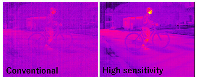
Consequently, the new sensor presents a sensitivity of more than three times the sensitivity of uncooled infrared image sensors using vanadium oxide or amorphous silicon, which are currently the mainstream materials.
In addition, a new device structure was developed by combining the thermal separation structure utilized in conventional uncooled infrared image sensors, Micro Electro Mechanical Systems (MEMS) device technology employed to realize this structure and CNT printing and manufacturing technology developed over several years (including that used for printed transistors). This successful integration resulted in the development of a high‐definition uncooled infrared image sensor with a 640 × 480‐pixel array.
NEC will continue its research and development efforts to further improve the developed infrared image sensor and create products and services that can be applied across various fields and areas of society.
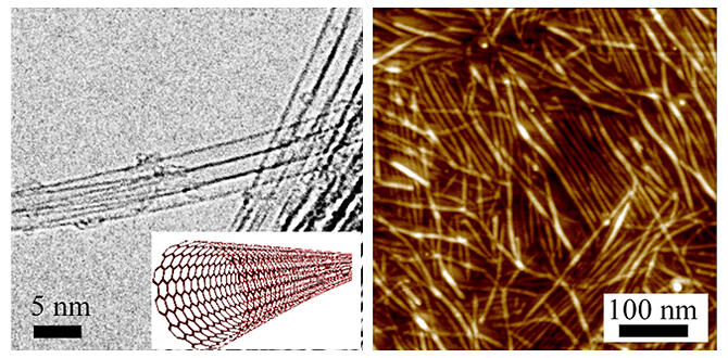
(Right) Atomic microscope image of a high‐purity semiconducting CNT film
Provided by NEC
Some of the results of this study were obtained in collaboration with the National Institute of Advanced Industrial Science and Technology (AIST). In addition, the study also received support from the National Security Technology Research Promotion Fund JPJ004596 implemented by the Japanese Government's Acquisition, Technology & Logistics Agency (ATLA).
This article has been translated by JST with permission from The Science News Ltd. (https://sci-news.co.jp/). Unauthorized reproduction of the article and photographs is prohibited.