
A collaborative research group led by Associate Professor Shinya Yamada, Graduate Student Masatoshi Kato (at the time of the research), and Professor Kohei Hamaya at the Graduate School of Engineering Science of Osaka University, in conjunction with Assistant Professor Shuhei Ichikawa and Professor Yasufumi Fujiwara at the Graduate School of Engineering of Osaka University, successfully fabricated a high‐performance spintronics material (Heusler alloy magnet) on GaN, a highly promising semiconductor material developed in Japan. Furthermore, the research group developed the technique of high‐efficiency spin injection through low‐resistance junctions at room temperature, using an electrode structure comprised of a high‐performance magnet and GaN. Their research was published in Advanced Electronic Materials.
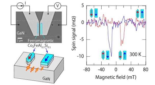
(b) Representative nonlocal spin signal measured at room temperature.
Provided by Osaka University
GaN is widely applied in various fields, such as optoelectronics and power electronics. Moreover, its application is expected to be expanded into the field of spintronics, actively utilizing the spin degree of freedom of electrons. Notably, GaN is an attractive semiconductor material for spin‐emitting devices.
However, most previous research generally employed a high‐resistance electrode structure utilizing an insulator tunnel barrier layer (ferromagnet/insulator tunnel barrier/GaN) for spin injection from a ferromagnet to GaN. These methods face practical challenges, such as requiring high voltages for device operation and relatively low‐efficiency spin injection, which directly affect the device performance.
To achieve low‐power consumption and high‐efficiency spin injection into GaN, the research group utilized Heusler alloy magnets as the spin injection source material and employed Schottky tunneling contacts with GaN. Heusler alloy magnets are efficient spin injection source materials for semiconductor materials such as gallium arsenide (GaAs) and germanium (Ge). However, due to significant differences in the crystal structure and the mismatched atomic arrangements on the surface, fabricating high‐quality Heusler alloy magnets on GaN has been extremely difficult.
The research group successfully achieved the epitaxial growth of Heusler alloy magnets on GaN by inserting a few atomic layers (approximately 0.4 nanometers) of cobalt (Co) at the interface between the materials to realize Schottky tunneling contacts. Furthermore, they were able to fabricate a test device structure using the electrode structure with Schottky tunneling contacts and successfully observed a spin injection signal at room temperature.
In the spin injection electrode structure, no insulator tunnel barrier layer is inserted between the high‐performance magnet and GaN. This achievement resulted in junction resistance values more than three orders of magnitude lower than that of conventional methods, enabling spin injection with low‐power consumption. A spin injection efficiency 3‐4 times higher than that obtained with conventional methods was also achieved by utilizing high‐performance Heusler alloy magnets as the spin injection source.
The research findings demonstrated "low‐power consumption and high‐efficiency" spin injection into GaN, which is expected to contribute to the realization of compact GaN‐based spin lasers driven by battery‐level low voltage in the future.
Yamada stated, "These research findings were made possible by collaboration with researchers in different fields. We started this collaborative research in 2018, and it took approximately five years to publish the paper. However, this is a very memorable and significant research achievement for me as it promotes interdisciplinary fusion research. I would like to express my gratitude to everyone involved once again and will continue my research to further develop these findings."
This article has been translated by JST with permission from The Science News Ltd. (https://sci-news.co.jp/). Unauthorized reproduction of the article and photographs is prohibited.