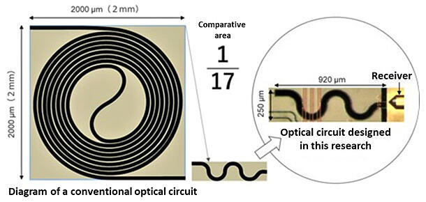
KDDI Research, Inc., and Waseda University developed a prototype silicon optical circuit for an optical AI accelerator with an area that is approximately 1/17th of that of conventional ones to predict time‐series data, with an eye on achieving low power consumption and high‐speed AI.

Provided by KDDI Research, Inc.
The two parties will continue to explore and scale up the structure of optical circuits. The objective is to enable the use of optical AI accelerators in a wide range of scenarios and establish the fundamental technology for optical AI chips. These chips are expected to offer significantly lower power consumption, approximately one‐tenth that of GPU‐based AI accelerators, and high speed.
This accomplishment was showcased at CLEO 2023 (Conference on Lasers and Electro‐Optics), a prominent international academic conference on optoelectronics held in San Jose, California, USA. The announcement of this achievement was made on May 8.
Numerous computers are needed to operate state‐of‐the‐art AI, and the challenge is to reduce their power consumption while accelerating their processing speed. Commonly used AI operates on electronic circuits.
In contrast, optical AI accelerators, which replace some operations with optical circuits, have been the focus of considerable research and development because of their effectiveness in reducing power consumption and their ability to accelerate learning and inference, making them promising solutions to such AI problems.
Among these solutions, silicon‐based optical circuits are particularly promising due to their potential for seamless integration with electronic circuits and other optical components, as well as their ability to be miniaturized. However, to make optical accelerators practical, it is necessary to facilitate large‐scale integration and pursue further miniaturization.
The silicon optical circuit for optical AI accelerators developed by the two companies, which has an area approximately 1/17th that of conventional circuits, is a prototype measuring 0.25 mm × 0.92 mm.
To evaluate its performance, the group used it to predict the Santa Fe waveform, which is a standard task. It was found that the error between the correct and predicted data was small, indicating the effectiveness of its structure. Optical circuits formed on silicon, which have been studied in the past, need to mix present and past information to perform reservoir computing—one of the models of AI—and have adopted one of the following structures.
The first is a structure that mixes present and past information repeatedly using optical circuits that form a network of signals. To ensure effective mixing timing, the distance between the nodes of the network must be maintained, resulting in a large element area (16 mm²). Increasing the number of neurons (the number of nerve cells) necessitates a larger area.
The second is a long spiral‐shaped multimode optical waveguide structure. A long (approximately 4 cm) optical waveguide is needed to mix present and past information using the properties of a multimode optical waveguide, in which many light waves can travel at different speeds. Approximately 2 mm × 2 mm is required even if the optical guide is stored in a spiral shape.
In this prototype, the waveguide width is twice that of the second structure, and the length is further tuned using a serpentine waveguide structure to generate many light waves (higher‐order modes) that travel slowly with a small waveguide length. The signal is designed to be sufficiently fast to mix present and past information.
This article has been translated by JST with permission from The Science News Ltd. (https://sci-news.co.jp/). Unauthorized reproduction of the article and photographs is prohibited.


