In recent years, microfabrication technology for semiconductor nanotechnology has almost reached its developmental limits. The 'top-down method,' in which circuits are fabricated by scraping the surface of the material, is difficult to use to create quantum-fine wire patterns with widths and spacings of less than 10 nanometers (one-billionth of a meter). On the other hand, the 'bottom-up method,' in which the design and synthesis of fine wires are made from scratch, enables the design of fine wires in the atomic size range. However, the fabrication and arrangement of uniform fine wires using this method is a major challenge.
A research group led by Program-Specific Associate Professor Tomoya Asaba and Professor Yuji Matsuda of the Graduate School of Science at Kyoto University, has focused on the 'Turing patterns,' spatial patterns that spontaneously appear when two substances react and diffuse, such as the stripes on a tropical fish or the spots on a panther. Ruthenium chloride thin films were deposited on graphite substrates using 'pulsed laser deposition,' a thin-film deposition method in which a laser beam is repeatedly applied to a material for a short period of time to deposit it on a substrate.
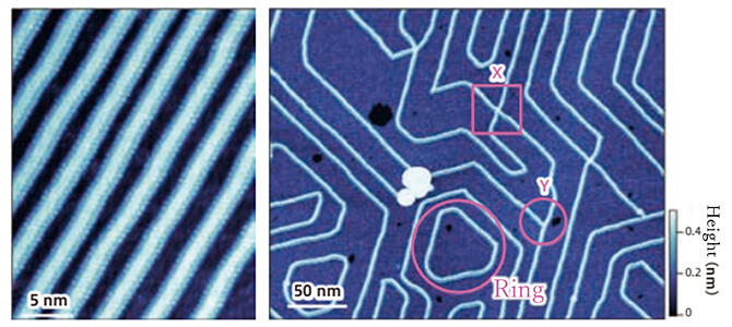
Scanning tunneling microscopy (STM) revealed a structure composed of periodically aligned ruthenium chloride quantum wires. These quantum wires are extremely thin, with a thickness and width of approximately one nanometer but lengths exceeding one micrometer (one-millionth of a meter). The width and spacing of the wires could be adjusted by changing the deposition time and substrate temperature to form not only stripes but also X, Y, and ring patterns.
This achievement opens up a new perspective on ultrafine fabrication in nanotechnology, leading to applications such as quantum circuits, light-sensitive devices, and atomic coils based on pattern formation. From a basic research perspective, it also provides an interesting framework for the search for novel physical phenomena.

Large-area STM image of quantum wires forming X- and Y-shaped junction rings (right).


