
On September 5, 2023, OKI, in collaboration with Shin-Etsu Chemical, announced the successful development of a technology that uses OKI's crystal film bonding (CFB) technology to peel off only the gallium nitride (GaN) functional layer from Shin-Etsu Chemical's uniquely improved Qromis Substrate Technology (QST) substrate and bond it to a different material substrate. This technology enables the vertical conduction of GaN and is expected to contribute to the realization and commercialization of vertical GaN power devices capable of controlling large currents. The two companies will work further together to develop vertical GaN power devices that can be implemented in society by partnering with companies that manufacture these devices.
Provided by OKI
GaN devices are attracting attention as next-generation devices that combine high device characteristics with low power consumption, such as power devices that require high breakdown voltages of 1800 volts or more, high-frequency devices for Beyond5G, and high-brightness micro-LED displays. In particular, vertical GaN power devices are expected to achieve significant demand growth as devices that can improve the basic performance of electric vehicles by endowing them with extended driving ranges and shortened power supply times. However, two major challenges hinder the social implementation of vertical GaN power devices: the diameter of the wafers must be increased to improve productivity and vertical conductivity must be realized to enable large current control.
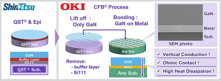
Shin-Etsu Chemical's QST substrate, which the company licensed in 2019, is a composite material substrate developed by Qromis, a US company dedicated to GaN growth. Because the coefficient of thermal expansion of this substrate is equivalent to that of GaN, it can suppress warpage and cracking. This characteristic enables the crystal growth of thick GaN films with high breakdown voltages even on wafers larger than 8 inches, thereby enabling the production of wafers with larger diameters.
On the other hand, OKI's CFB technology was developed to peel off the crystal film from the growing substrate and bond it to a substrate made of a different material. The CFB technique can exfoliate only the GaN functional layer from the QST substrate while maintaining high device characteristics. The insulating buffer layer required for GaN crystal growth can be removed and bonded to various substrates via metal electrodes that allow electrical bonding (ohmic contact) with a linear current−voltage curve according to Ohm's law. Bonding of these functional layers to a conductive substrate with high heat dissipation will enable both high heat dissipation and vertical conductivity. Through this, the combined technologies of Shin-Etsu Chemical and OKI solve the above two problems, paving the way for the social implementation of vertical GaN power devices.
In the future, the two companies will contribute to the realization and widespread use of vertical GaN power devices through Shin-Etsu Chemical's provision of QST or epitaxial substrates to companies manufacturing GaN devices and OKI's provision of CFB technology through partnering and licensing. Furthermore, OKI hopes to use CFB technology to provide added value to semiconductor devices that go beyond the framework of single materials and help realize the company's key message of "making society safe." Shin-Etsu Chemical also presented this technology at "SEMICON Taiwan," a seminar held in Taipei from September 6 to 8, 2023.
This article has been translated by JST with permission from The Science News Ltd. (https://sci-news.co.jp/). Unauthorized reproduction of the article and photographs is prohibited.