
A research group led by Assistant Professor Kou Li, Professor Yukio Kawano, and Graduate Student Yuto Matsuzaki of the Department of Electrical, Electronic, and Communication Engineering at the Faculty of Science and Engineering at Chuo University announced their successful development of an exceptionally efficient manufacturing process. They achieved this through the utilization of printing technology to fabricate their proprietary multifunctional 'optical and electromagnetic wave imaging sensor sheet.' The research group devised a fabrication process in which each material, in its liquid ink state, is imprinted with high adhesion using printing technology. This process mitigates element disconnections and malfunctions, leading to a significant enhancement in fabrication efficiency and overall durability. The results are expected to pave the way for the practical implementation of highly durable sensor sheets characterized by high fabrication efficiency. The results were published in the international journal Advanced Materials Interfaces on September 22.
Provided by Chuo University
With the advent of the IoT society, demand for non-destructive inspection technology is rapidly increasing. There is a growing sense of anticipation for optical and electromagnetic wave imaging technology, which can acquire inspection data over extensive areas without physical contact.
In particular, light and electromagnetic waves, including millimeter waves, terahertz waves, and infrared radiation, all of which are situated within the spectrum between visible light and radio waves, are expected to assume a pivotal role in non-destructive testing technology because they can identify non-metallic materials, which constitute a significant portion of industrial products and infrastructure.
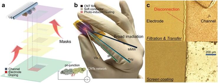
To date, the research group has studied non-destructive testing devices and systems operating within the same frequency band. Among these endeavors, the research group achieved a significant milestone by utilizing carbon nanotube (CNT) thin film as the element material. They successfully developed the world's first ultra-broadband and highly sensitive millimeter-wave-infrared band imaging sensor sheet with thin, soft, and stretchable characteristics. However, disconnections frequently occur between the CNT film of the sensor component and the electrode wiring responsible for signal readout during device fabrication. This issue has emerged as a concern for future endeavors in large-scale integration.
The research group initially worked to determine the cause of these disconnections and found that they were caused by peel-off transfer, a conventional CNT film processing method. Subsequently, as an alternative to the peel-off transfer process, a novel approach was implemented, which involved the adoption of a screen-printing method. This innovation took inspiration from the coating method of imprinting ink on partial holes, similar to the practices found in printmaking and T-shirt printing. The film quality and thickness can be managed by adjusting the ink viscosity, while the size of the selectively formed CNT film can be controlled during the design stage of the coating window. Furthermore, it was confirmed that this screen-printing method yields a remarkable improvement in durability compared to the conventional tendency of wires breaking at the electrode interface.
As the culmination of these highly durable and high-yield device fabrication processes, the research group has succeeded in the integration of multiple CNT film imaging elements through screen printing techniques. These integrated elements have found practical application in non-destructive inspection devices. In the future, they aim to venture into the domain of screen printing for camera sheets, with the goal of achieving high-density, large-scale integration of CNT film-type pixels on a two-dimensional plane. This endeavor is expected to evolve into the development of video camera-type real-time inspection video imaging systems, transcending the current demonstration of non-destructive inspection that relies on still image imaging.
In addition to the screen printing of CNT dispersion liquid and conductive paste, the research group has demonstrated the screen printing of doping liquid, a crucial component for achieving high-sensitivity optical and electromagnetic wave detection. Furthermore, they have also demonstrated the screen printing of insulating paste, essential for facilitating the three-dimensional cross-wiring of electrodes, making it suitable for complex integrated structures required in camera production.
Li said, "Given the increasing demand for non-destructive testing, easy handling of the testing elements has emerged as an equally critical consideration alongside the high-performance attributes of these elements. The focus of this research was to answer the simple question, 'What kind of fragile element is this?' We were able to solve this question and establish a simple fabrication process that demands no specialized user skills. We will continue to prioritize both high performance and user-friendliness as we strive to create original cameras that contribute to society."
Journal Information
Publication: Advanced Materials Interfaces
Title: All-Screen-Coatable Photo-Thermoelectric Imagers for Physical and Thermal Durability Enhancement
DOI: 10.1002/admi.202300528
This article has been translated by JST with permission from The Science News Ltd. (https://sci-news.co.jp/). Unauthorized reproduction of the article and photographs is prohibited.