
As 2D sheets (two-dimensional materials) with a thickness equal to that of an atom, such as sheets of graphene, transition metal dichalcogenides (TMDs), and hexagonal boron nitride (hBN), possess unique properties, they are expected to be developed into next-generation semiconductors, superconductors, flexible electronics, and various types of sensors. However, transferring 2D sheets onto substrates presents several challenges, including breakage of 2D materials or performance degradation due to the presence of polymer residue in the protective film.
A research group led by Distinguished Professor Hiroki Ago of the Global Innovation Center at Kyushu University, Nitto Denko Corporation, the Institute for 2D Materials LLC., Assistant Professor Kou Li and Professor Yukio Kawano at Chuo University, Professor Kazunari Yoshizawa of the Institute for Materials Chemistry and Engineering at Kyushu University, Associate Professor Yuta Tsuji of the Interdisciplinary Graduate School of Engineering Sciences at Kyushu University, Professor Kazutomo Suenaga of the Institute of Scientific and Industrial Research at Osaka University, and Principal Researcher Yung-Chang Lin of the National Institute of Advanced Industrial Science and Technology (AIST) has developed a functional tape whose adhesive strength decreases under UV irradiation. This tape is specialized for 2D materials that can address the aforementioned issues. As this tape can be used for various 2D materials, the group has also fabricated a flexible terahertz sensor on a trial basis. Ago stated, "We aim to advance the development of next-generation 2D semiconductor applications by around the year 2030, in collaboration with semiconductor device manufacturers." The results were published in the online edition of Nature Electronics.
Credit: Ago Lab, Kyushu University
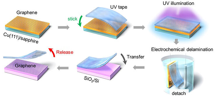
When fabricating 2D materials such as graphene on a silicon substrate, a copper catalyst is deposited onto a sapphire substrate, and graphene is synthesized on top of it. After coating the surface with a polymer protective film, the material is immersed in an etching solution to dissolve the copper, enabling the transfer of the graphene remaining on the polymer film onto the silicon substrate. However, this method requires approximately 3 days and presents certain challenges, including the difficulty of achieving large areas due to the fragility of polymers, polymer residues, and inability to recycle copper in catalysts.
Intrigued by the possibility of easily attaching materials using tape, Ago and colleagues initiated joint research with Nitto Denko in 2017. In this study, they developed a transfer tape and process that reduce adhesive strength to one-tenth of the original value upon exposure to UV light.
In this novel process, graphene is formed on a copper catalyst, and tape is attached to it. Upon exposing the tape to UV light, hydrogen is generated electrochemically between graphene and copper, causing the graphene on the tape to peel off from the copper catalyst. The tape is placed on a silicon substrate, and after applying certain pressure, the tape is peeled off, leaving only graphene on the silicon substrate. Without using solvents, copper can be recycled and transferred onto materials such as plastic.
Graphene transfer rates of up to 99% (minimum 95%) were achieved in ten tests. Almost no polymer residue and nearly no graphene breakage was observed. Further, the electron mobility of the graphene device increased by 33% compared to that achieved using the conventional method.
The primary component of the tape adhesive, a random copolymer, contains double bonds. Upon exposure to UV light, a polymerization reaction occurs, causing a reduction in van der Waals forces. Furthermore, the adhesive hardens under UV irradiation, concentrating shear stress at the interface between the substrate and adhesive. This process enables the delicate transfer observed in this study. Ago stated, "We created training data by combining multiple materials and analyzed them with AI to determine the optimal tape and transfer process. Controlling van der Waals forces was a trial-and-error process, leading to considerable challenges."
The research group succeeded in attaching 2D materials to not only graphene but also hBN and TMD. Moreover, it succeeded in forming a bilayer structure of graphene and hBN. The group also realized the transfer of graphene with a current maximum diameter of 10 cm and expects to transfer even larger materials in the future with the development of device manufacturers' technology.
Ago stated, "We will promote the practical application of 2D materials through proactive collaboration with numerous universities and companies in industry− academia partnerships."
Journal Information
Publication: Nature Electronics
Title: Ready-to-transfer two-dimensional materials using tunable adhesive force tapes
DOI: 10.1038/s41928-024-01121-3
This article has been translated by JST with permission from The Science News Ltd. (https://sci-news.co.jp/). Unauthorized reproduction of the article and photographs is prohibited.