
Light in the near-infrared (NIR) region is expected to be applied to a wide variety of fields, including optical communications (wavelengths between 1310 and 1550 nm) and sensing with eye-safe lasers (wavelengths of 1400 nm and above) that are beyond human sensory perception. However, silicon-based digital cameras cannot use NIR light owing to limitations imposed by the bandgap. Additionally, InGaAs (Indium Gallium Arsenide) cameras, which cost over a million yen, are too expensive for wide social implementation.
A research group led by Professor Hiroshi Kitagawa and Program-Specific Associate Professor Kohei Kusada of the Graduate School of Science at Kyoto University and Senior Researcher Shinya Okamoto at Panasonic Holdings Corporation's Technology Division has successfully developed a plasmonic Schottky device in which a gold-silver (AuAg) nanoalloy is formed on a silicon substrate. This device improves the photoelectric conversion efficiency in the NIR region corresponding to optical communication and eye-safe wavelengths. Okamoto commented "by controlling the pulse frequency of arc plasma, we were able to easily form plasmonic nanostructures in a very short time of approximately 1 min. Since we have successfully demonstrated a new concept this time, we plan to further advance our research and expand the application of these structures to various devices in the future." The results were published in ACS Applied Materials & Interfaces.
Provided by Kyoto University
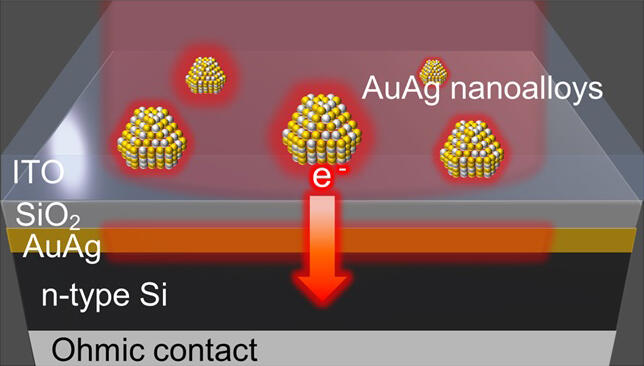
In photoelectric conversion using a plasmonic Schottky device, light is first absorbed through plasmon resonance, which raises electrons to a high-energy state. When these electrons overcome the Schottky barrier at the interface between the semiconductor and metal nanoparticles, they are accelerated and result in the production of a current. Various research groups have been advancing the development of plasmonic Schottky devices, mainly through approaches such as the fine processing of nanostructures using techniques like lithography to enhance plasmon absorption in the NIR region. However, these conventional approaches are too costly to be practical. About five years ago, Okamoto thought, "If we lower the Schottky barrier to the appropriate height, might it be possible to extract electrons?" This was the starting point of the research.
The Schottky barrier height is determined by the work function of the metal and the affinity of the semiconductor. Therefore, a combination of Au (high work function) and Ag (low work function) was employed. To control the Schottky barrier precisely, metal and silicon must be joined directly. For the first time, the research group used the arc plasma deposition method. Removing the natural oxide film from silicon and applying 40 pulses of arc plasma to the flat and clean silicon surface at the atomic level results in the formation of an AuAg alloy layer. Simultaneously, silicon diffuses from the silicon surface onto the alloy layer, forming an amorphous silicon layer. After growing the amorphous silicon layer to a thickness less than 2 nm, AuAg alloy nanoparticles were formed on it. This process took approximately 1 min.
According to the survey on the optical properties of the device, the AuAg nanostructures on the surface demonstrated plasmon absorption in the NIR region. When irradiated with NIR light of the kind used in optical communication, a photocurrent was generated, even though the bandgap energy of silicon was not reached. Furthermore, when devices with varying composition ratios (Au:Ag) were fabricated and examined for their light response, the observed photocurrent increased with an increase in the proportion of Ag. The device with a composition of 40:60 achieved the maximum photocurrent. This result indicates that the Schottky barrier can be controlled via the composition ratio. The uniformity of the Schottky barrier over the entire silicon substrate, arising from the formation of the AuAg film, also contributed to the improved photoelectric conversion efficiency.
Consequently, the internal quantum efficiency of the fabricated device was found to be 4.6 and 6.5 times higher at wavelengths of 1310 and 1550 nm, respectively, a significant improvement over a previous study.
Okamoto commented, "We are working towards realizing applications of NIR light by enhancing plasmonic absorption and further improving sensitivity. Additionally, in photoelectric conversion, we aim to explore extending the utilization of light energy below the semiconductor bandgap to expand applications to various fields beyond photodetection, such as photocatalysis."
Journal Information
Publication: ACS Applied Materials & Interfaces
Title: Facilely Fabricated Zero-Bias Silicon-Based Plasmonic Photodetector in the Near-Infrared Region with a Schottky Barrier Properly Controlled by Nanoalloys
DOI: 10.1021/acsami.3c15328
This article has been translated by JST with permission from The Science News Ltd. (https://sci-news.co.jp/). Unauthorized reproduction of the article and photographs is prohibited.