
Magnetic materials include ferromagnetic materials, where magnetization occurs at the macroscopic level, and antiferromagnetic materials, which are magnetic at the atomic level but not at the macroscopic level. Ferromagnetic materials have been used to date in spintronics for nonvolatile information storage. However, if the spin of antiferromagnetic materials can be utilized, it is possible to achieve device operating speeds in the terahertz range, which are two to three orders of magnitude higher than those of the devices made using ferromagnetic materials. Research and development in this regard is being conducted worldwide.
A joint research group including Associate Professor Yu Shiratsuchi, Graduate Student Kakeru Ujimoto (at the time of research) and Graduate Student Hiroki Sameshima from the Graduate School of Engineering at Osaka University, Professor Takahiro Moriyama from the Graduate School of Engineering at Nagoya University, Professor Kohji Nakamura from the Graduate School of Engineering at Mie University, Professor Motohiro Suzuki from the School of Engineering at Kwansei Gakuin University, and Senior Researcher Naomi Kawamura from the Japan Synchrotron Radiation Research Institute (JASRI) has developed a voltage-based spin-control technique for antiferromagnetic chromium oxide Cr2O3 thin films that can be driven at high speeds with low power consumption. The group has also succeeded in increasing the spin-control efficiency to more than 50 times higher than conventional ferromagnetic materials. The research results were published in NPG Asia Materials.
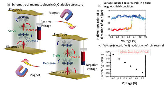
(b) The signal (Hall voltage) changes due to spin inversion when only the voltage is changed in a fixed magnetic field.
(c) Modulation of the switching field according to the applied voltage.
Provided by Osaka University
The research group recently demonstrated that it is possible to control the spin of antiferromagnets by thinning Cr2O3 layers to the nanometer scale, where a strong spin effect is present. To achieve this phenomenon in real devices, it is necessary to control the voltage required for low-power drive. However, the material properties that can be controlled through voltage are dielectric properties, and the magnetic properties unique to magnets cannot be directly controlled by voltage. As a result of this the group focused on the electromagnetic effect (the combined effect of magnetism and dielectricity). This effect is caused by the movement of magnetic ions within a crystal due to voltage (dielectricity), which changes the spin state of the magnetic ions, and is applicable to antiferromagnetic materials.
The research group attempted to use this effect to control the spin of Cr2O3 thin films through variations in the voltage. As a result, they found that the spin direction of an antiferromagnetic material can be reversed by changing only the voltage without changing the magnetic field. The spin-reversal conditions can be changed by varying the voltage and magnetic field strength, and the spin-control efficiency is more than 50 times higher than that achieved for conventional ferromagnetic materials. They also clarified that the spin direction can be set using the voltage direction, demonstrating the possibility of future memory operations.
To explain the origin of this phenomenon, the research group performed element-selective magnetic measurements (X-ray magnetic circular dichroism measurements) at the large synchrotron radiation facility SPring-8. The research group revealed that the spin of chromium at the bonding interface with the Cr2O3 electrode metal (Pt) is reversed and plays an important role in controlling magnetism through electromagnetic effects. It was also revealed that the magnetic effect of the Pt film itself, which is observed in ferromagnetic materials, is negligibly low, indicating that the observed highly efficient spin control is achieved by a mechanism different from that observed in conventional ferromagnetic materials.
Furthermore, it has been thought that the electromagnetic effect occurs only in special magnetic materials. However, theoretical considerations based on first-principles calculations and experimental results show that the electromagnetic effect can be induced at the bonding interface between antiferromagnets and metals by a mechanism different from that observed within crystals. The research group also presented guidelines for the application of this effect to other materials.
The driving force necessary to change the orientation of magnetization must exceed the switching energy barrier that fixes the orientation. The driving force is determined by the product of magnetization and magnetic field. In antiferromagnetic materials, there is almost no driving force because there is no magnetization. This is the reason for the assumption is that "the spin of antiferromagnets cannot be controlled." Research is underway to lower the switching energy barrier of ferromagnetic materials through voltage application.
The electromagnetic effect that the research group focused on involves temporary generation of macroscopic magnetization through voltage application, and this effect elicits the driving force required for reversing magnetization. The research group has demonstrated that this effect can be used to control the spin of antiferromagnetic materials, which do not have inherent magnetization, and the spin direction can be controlled with high efficiency using a different principle from that associated with ferromagnetic materials. This discovery presents guidelines to achieve spin control in antiferromagnets and design materials for voltage-driven spintronic devices in the future.
Journal Information
Publication: NPG Asia Materials
Title: Giant gate modulation of antiferromagnetic spin reversal by the magnetoelectric effect
DOI: 10.1038/s41427-024-00541-z
This article has been translated by JST with permission from The Science News Ltd. (https://sci-news.co.jp/). Unauthorized reproduction of the article and photographs is prohibited.