There are great expectations for the realization of next-generation ultra-low power memory and computing devices based on ferroelectric materials, such as memories with power consumption less than 1/100th of the current level, and brain-inspired computers, which are currently under development. A deep understanding of nanoscale polarization inversion phenomena is essential to improve the reliability of these devices. A research group led by Associate Professor Yoshiomi Hiranaga of the Research Institute of Electrical Communication at Tohoku University and Specially Appointed Professor Yasuo Cho of the New Industry Creation Hatchery Center, in collaboration with a research group led by Professor Hiroshi Funakubo of the Department of Innovative and Engineered Materials at the Interdisciplinary Graduate School of Science and Engineering at Tokyo Institute of Technology, has developed a new microscopy technique. This technique enables the observation of polarization reversal behavior in ferroelectric materials with nanoscale spatial resolution and high-definition images in a short period of time (1/300th of conventional methods). This is expected to advance our understanding of phenomena that hinder device reliability and promote improvements in material properties based on this knowledge. The research was published in ACS Applied Nano Materials.

Provided by the Research Institute of Electrical Communication (RIEC), Tohoku University
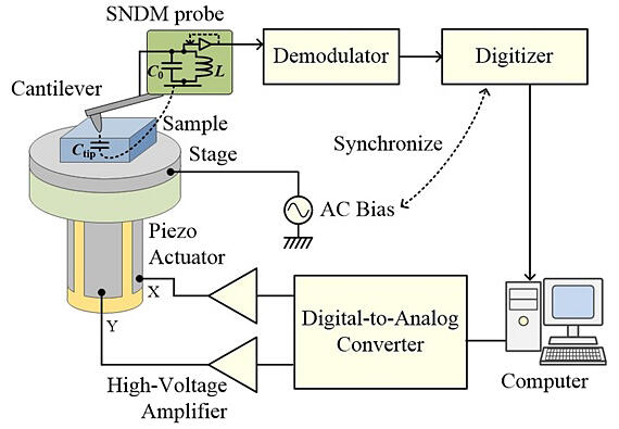
The problem of ferroelectric materials is polarization fatigue, which causes the amount of polarization to gradually decrease after numerous repetitions of polarization reversal operations (corresponding to rewrite operations in memory devices). To suppress this and improve device reliability, it is necessary to better understand the polarization reversal behavior in the micro-region and improve material properties based on this knowledge. The research group developed a new microscopy technique called local C-V mapping. This technique uses a scanning nonlinear dielectric microscope (SNDM), a modified version of the probe microscope.
The sensing part of the SNDM comprises an extremely sharp probe with a nanoscale size tip and a high-sensitivity capacitance sensor, which can measure the slight capacitance change (or dielectric constant change) that occurs when a bias voltage is applied to the measurement sample. It is known that a characteristic capacitance-voltage (C-V) curve called a butterfly curve is drawn when capacitance is measured while an AC bias voltage with an amplitude exceeding the polarization reversal voltage is applied to a ferroelectric sample. Such C-V curve is usually measured using an electrode of approximately 0.1-1-mm diameter. Meanwhile, the extremely high measurement sensitivity of the SNDM probe allows similar measurements to be made using nanometer-sized electrodes.
In fact, by analyzing the peak positions and peak areas of the C-V curves obtained from measurements of lithium tantalate single crystals, they could extract information on the polarization inversion behavior. Additionally, the probe can be moved using a fine actuator (piezo actuator), which allows measurements to be taken at each point, resulting in two-dimensional image-like data. Such measurements allow direct observation of, for example, in-plane variations in polarization reversal voltage. Through this, it becomes possible to capture in real space where and to what extent factors that inhibit polarization inversion, such as crystal defects, are unevenly distributed. A similar measurement method that has been proposed is based on a method of detecting piezoelectric response − i.e., the mechanical response when voltage is applied to a measurement sample (piezoelectric response microscope). However, the new method succeeded in reducing the measurement time to approximately 1/300th of the conventional method. High-resolution observation data that would require several days for a single measurement with conventional methods can now be acquired in approximately 10 minutes using the new method.
The group also introduced machine learning to the analysis of the obtained measurement data and developed a method to display the distribution of polarization reversal behavior in an image format. In the experiment, hafnium oxide-based thin films were measured, and using a machine learning technique called clustering, regions showing similar polarization inversion behavior were automatically identified and colored. From the data, it is possible to determine the distribution of regions where polarization reversal occurs at low voltages, regions where reversal requires high voltages, regions where asymmetry in reversal behavior is observed due to factors that inhibit polarization reversal, and regions where polarization reversal does not occur at all. Furthermore, this measurement system can simultaneously acquire surface profile images in the same observation area. By comparing these with local C-V map data, it is possible to directly and thoroughly investigate, for example, how and to what extent grain boundaries affect the polarization inversion behavior. These developments will advance our understanding of polarization fatigue in various ferroelectric materials. Moreover, combining this technique with another probe microscope is expected to facilitate multifaceted analysis.
Journal Information
Publication: ACS Applied Nano Materials
Title: Data-Driven Analysis of High-Resolution Hyperspectral Image Data Sets through Nanoscale Capacitance-Voltage Measurements to Visualize Ferroelectric Domain Dynamics
DOI: 10.1021/acsanm.3c04636
This article has been translated by JST with permission from The Science News Ltd. (https://sci-news.co.jp/). Unauthorized reproduction of the article and photographs is prohibited.


