
A research group led by Professor Tadatomo Suga and Senior Researcher Junsha Wang of the Meisei University Collaborative Research Center in collaboration with Professor Kazuya Yamamura of the Research Center for Ultra-Precision Science & Technology, Graduate School of Engineering at Osaka University, and IIPT Inc. has successfully processed a large-diameter diamond substrate into an ultrasmooth surface with a roughness of 0.5 nm or less and bonded it to a GaN wafer and piezoelectric single-crystal wafer at room temperature for the first time in the world. This achievement is a major step toward the practical application of high-efficiency power devices and was presented at the International Conference 2024 IEEE 74th Electronic Components and Technology Conference.
Provided by Meisei University
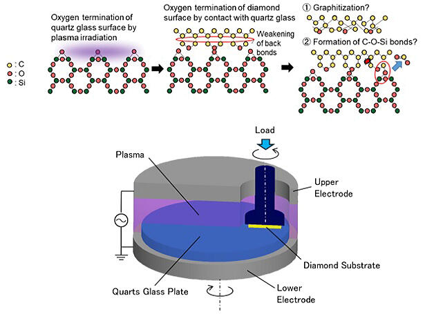
Increased heat generation due to miniaturization, together with higher integration, performance, and output of power devices has become an issue in recent times. Diamond is an ideal material for heat dissipation, but smoothing it at the nano level, which is required for it to bond with semiconductors, is challenging. Synthetic diamond can be created using the chemical vapor deposition (CVD) method. However, as its area increases, the wafer may warp, which must be corrected and then polished to achieve ultrasmoothing. As a result, although small laboratory-scale power devices can be fabricated, practical bonding at the inch-scale has not been possible.
After two years of joint research involving the application of the plasma-assisted polishing (PAP) process developed by Yamamura and his colleagues at Osaka University, Suga succeeded in polishing a 2-inch diamond wafer for the first time and reducing its warping to about 2 microns. Furthermore, in collaboration with IIPT, Suga succeeded in further smoothing the diamond wafer after PAP by optimizing gas species and beam-irradiation conditions for gas-cluster ion-beam processing (GCIB) to obtain an ultrasmooth surface roughness at the 0.5-nm scale. The diamond wafers were successfully bonded to a 2-inch-diameter GaN substrate and a 4-inch-diameter piezoelectric single-crystal (lithium niobate) substrate at room temperature.
Suga said, "Several steps are needed for this technology to be practically used by companies, including further enlargement of the diameter, but they are not that difficult. Rather, the fact that diamond deposition is not being done domestically will be a challenge for mass production."
This article has been translated by JST with permission from The Science News Ltd. (https://sci-news.co.jp/). Unauthorized reproduction of the article and photographs is prohibited.