On July 4, Hitachi, Ltd., Kyushu University, RIKEN, and HREM Research Inc. announced that, in collaboration with the National Institute for Advanced Industrial Science and Technology (AIST) and the National Institute for Materials Science (NIMS), they had developed a method that enables the observation of magnetic fields in structures such as magnetic multilayers and samples with non-uniform compositions, on individual lattice planes. The research group used Hitachi's atomic-resolution holography electron microscope to achieve, for the first time in the world, the aforementioned observation that had been difficult in the past. The results were published online the same day in the international academic journal Nature.

Provided by Hitachi, Ltd. Research & Development Group
Many electronic devices and motors used in smartphones, computers, automobiles, trains, etc., owe much of their function and performance to the arrangement of atoms, the smallest unit of matter, and the behavior of their electrons. Therefore, technology to observe materials at ultrahigh resolution at the atomic level has become important for the development of new functionality and further performance improvement in such devices and machinery. To this end, Hitachi has been developing holography electron microscopes since 1966 to directly observe electric and magnetic fields in minute regions of materials, and it developed an atomic-resolution holographic electron microscope in 2014. Its resolution was further improved; in 2017, in collaboration with RIKEN, and a sub-nanometer (1 nm or below) resolution was achieved, which enables magnetic field observation of several layers of atoms. However, there were problems to be resolved for achieving higher resolution: improvement of the precision of the microscope and correction of minute focal shifts that occur during imaging. Higher resolution was not achieved as these problems remained unresolved.
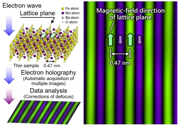
To resolve these issues, the research team has succeeded in developing a technique to observe the magnetic field of each lattice plane for non-uniform samples such as magnetic multilayers, which had been difficult to observe in the past. Furthermore, the research team addressed previous challenges by improving the accuracy of electron holography and developing a technique to automatically correct the focus after imaging. First, they improved the accuracy of electron holography by increasing the number of image data to be acquired. The research group has developed a technology that can automatically capture over 10,000 images in approximately 8.5 hours while maintaining ultrahigh resolution by automatically controlling and adjusting the microscope and speeding up the imaging process during data acquisition. This technology is based on previous developments in 2017: separating electric field and magnetic field information with high accuracy using the observation results of electron beam holography. However, to achieve higher resolution, a technology to correct minute focus deviations in the imaging data is needed.
This concept of correcting the focus after imaging was the motivation for the invention of electron holography by British physicist Dennis Gabor in 1948, and it is a well-established theory. However, until now there had been no technology that automatically corrects these deviations. In this study, the research team applied, to electron holography, a method to correct the focus by analyzing electron waves obtained by changing the focus. They succeeded in automatically correcting the focus by developing a proprietary algorithm that reduces the effect of noise in the experimental data. They applied these techniques to Hitachi's atomic-resolution holography electron microscope to observe magnetic materials (Ba2FeMoO6 crystals) with magnetic fields of different sizes and orientations in each atomic layer. A comparison of the observation results with simulations confirmed that the magnetic field of each lattice plane inside the material could be observed with a resolution of 0.47 nm, the top of its class in the world for a method that can observe a nonuniform sample. This breakthrough has made it possible, for the first time in the world, to observe magnetic fields at the atomic layer level at the boundaries (interfaces) between local materials, which greatly affect the physical properties of materials including non-uniform samples and the characteristics of electronic devices.
The research team expects that this technology will contribute to the advancement of basic science through the elucidation of magnetic phenomena occurring at the atomic layer level. In addition, the research group is determined to contribute to developing high-performance magnets and high-performance materials for electrification to achieve decarbonization in pursuit of realizing a carbon neutral society as well as to developing energy-saving devices to reduce the overall consumption of energy in society.
Journal Information
Publication: Nature
Title: Electron holography observation of individual ferrimagnetic lattice planes
DOI: 10.1038/s41586-024-07673-w
This article has been translated by JST with permission from The Science News Ltd. (https://sci-news.co.jp/). Unauthorized reproduction of the article and photographs is prohibited.


