To process the explosively growing volume of data resulting from the development of information technology, including generative artificial intelligence, in real-time there is a strong demand for quantum computing methods that will fundamentally change information processing technology, along with substantially higher functionality, lower power consumption, and higher integration of existing devices. Topological superconductors have garnered considerable attention as an important material platform for realizing Majorana quasiparticles, a promising candidate for qubits in error-tolerant quantum computing.
The extensive research undertaken to date on topological superconductivity has exploited the proximity effect in hybrid structures of conventional superconductors and topologically nontrivial materials, such as topological insulators (TIs) and topological Dirac semimetals (TDSs). There are important requirements for realizing a material platform for large-scale quantum computing. These include the fabrication of high-quality interfaces between topological materials and superconductors, the simplicity and low cost of materials fabrication and device processing, and the possibility of nanoscale microfabrication. However, meeting these requirements has been very difficult in the past.
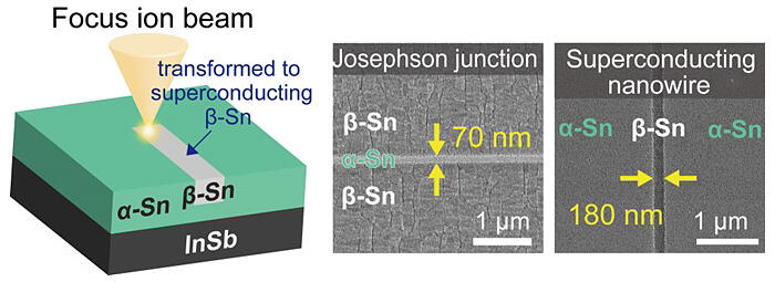
A new technology has been developed by a research group of Associate Professor Le Duc Anh, Associate Professor Masaki Kobayashi, Professor Masaaki Tanaka, Graduate Student (at the time of the research) Keita Ishihara, Graduate Student Tomoki Hotta, Graduate Student (at the time of the research) Kohdai Inagaki, Graduate Student Hideki Maki, and Graduate Student Takahiro Saeki of the Center for Spintronics Research Network at the Graduate School of Engineering of the University of Tokyo. The new technology developed by the research group is aimed at forming superconducting β-Sn nanostructures of arbitrary shapes at arbitrary positions within an α-Sn film by irradiating a TDS α-Sn thin film with an ion beam focused to a few nanometers and using the heat generated by ion collisions to cause a phase transition from α- to β-Sn.

A focused gallium ion beam (FIB) is irradiated to induce phase transition from topological Dirac semimetal α-Sn to superconducting metal β-Sn at arbitrary positions and in arbitrary nano-scale shapes (left). Scanning electron microscope (SEM) images some nanostructures fabricated using this method: a Josephson junction composed of β-Sn/α-Sn (70 nm width)/β-Sn fabricated (center), and a β-Sn superconducting nanowire (180 nm width) embedded in an α-Sn thin film plane (right).
Provided by the University of Tokyo
Using this technology, the researchers succeeded in fabricating a Josephson junction structure comprising superconductor β-Sn/TDS α-Sn (70 nm)/superconductor β-Sn, as well as a β-Sn nanowire (180-nm wide) structure embedded in an α-Sn film. The thermally formed interface between β- and α-Sn is atomically steep and has reduced impurity contamination, resulting in superior quality compared to that achieved using existing manufacturing methods. Furthermore, in the β-Sn superconducting nanowire embedded in the plane of an α-Sn film, when the direction of the current flow was changed while a magnetic field was applied parallel to the wire, the critical current of the superconducting nanowire substantially changed by 70%. In other words, when current flows through the nanowire in one direction, it enters a superconducting state with zero electrical resistance, and when current flows in the reverse direction, it enters a normal conducting state with nonzero electrical resistance. The nanowire functions as a superconducting diode element.
This superconducting diode effect is attributed to the topological electronic state of TDSα-Sn, which become superconducting due to the proximity effect near the interface with β-Sn. This is the first experiment to demonstrate the rich physical properties of a Sn-based superconductor/TDS heterojunction. The heterostructures comprising Sn-based superconductors and topological materials developed by the research group are easy to fabricate and have high-quality crystallinity and interfaces. They are expected to serve as platform materials for topological quantum arithmetic circuits to realize large-scale quantum computers. The results of the research were published in Nature Communications.
Journal Information
Publication: Nature Communications
Title: Large superconducting diode effect in ion-beam patterned Sn-based superconductor nanowire/topological Dirac semimetal planar heterostructures
DOI: 10.1038/s41467-024-52080-4
This article has been translated by JST with permission from The Science News Ltd. (https://sci-news.co.jp/). Unauthorized reproduction of the article and photographs is prohibited.


