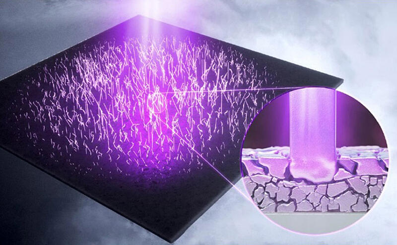
A Nagoya University group has succeeded in growing numerous "nanowires" with approximately 1/1000th the thickness of a hair on a thin aluminum film by irradiating it with ion beams. Pure-metal nanowires made of single crystals have few defects and high strength, and their optical properties make them promising for use in sensor devices and optoelectronics.

Provided by Associate Professor Yasuhiro Kimura, Kyushu University
Pure-metal nanowires are also called whiskers. Linear nanostructures with diameters ranging from 100 to 600 nm have garnered attention since around 2000 for their optical and electronic engineering properties such as surface light propagation, luminescence, and electron scattering.
According to Associate Professor Yasuhiro Kimura (materials mechanics, Graduate School of Engineering at Kyushu University), who conducted this research as Assistant Professor at the Graduate School of Engineering at Nagoya University, aluminum nanowires, among other metals, are expected to have applications in optical devices. However, the difficulty of mass-producing nanowires has been a challenge.
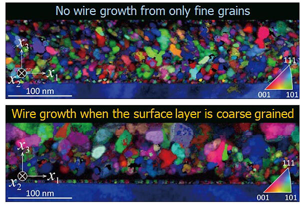
Kimura has been conducting research for approximately 10 years since he was a master's student. Initially, he studied a method of creating nanowires using electric currents, but there was a period of several years when they did not grow even under the right conditions. To investigate the cause, he observed thin films that produce nanowires under a microscope and noticed that the relatively large aluminum crystal grains inside the thin films seem to be necessary for nanowire growth.

Provided by Kimura
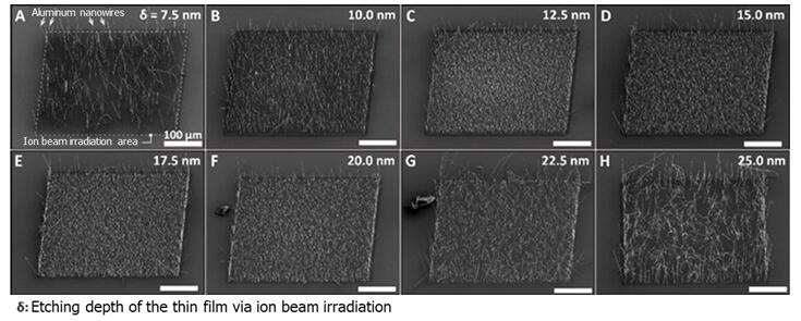
Believing that ion beam irradiation is an effective way to increase the size of crystal grains, Kimura and his colleagues irradiated a 100-nm-thick aluminum thin film with gallium ion beams. Nanowires then grew from the thin film like a forest full of trees. The nanowires were approximately 100-300 nm in diameter and 20-100 µm in length. A trade-off relation was observed between the nanowire density and length.

Provided by Kimura
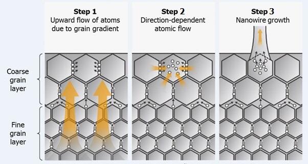
Focusing on the crystal grains inside the thin film, Kimura and his colleagues performed simulations of nanowire growth. Ion beam irradiation causes the crystal grains on the surface layer of the thin film to become larger and coarser, while the grains in the lower layers of the thin film remain fine. It is thought that the difference in the grain size creates a pressure gradient, which causes an upward flow of aluminum atoms, and that certain crystal grains act as crystal nuclei, which results in the atoms gathering and growing into single crystals that extend upward from the thin film, forming nanowires.

Provided by Kimura
Mass synthesis methods have been reported for nanowires of semiconductors, organic materials, and metal oxides. For pure-metal aluminum nanowires, the number density was reported in 1975 to be 200,000 per square centimeter when prepared via atomic diffusion, an atomic transport phenomenon in solids. However, it was demonstrated that this could reach 18 million using ion beam irradiation. Kimura commented, "This is expected to be the starting point for atomic-scale manufacturing technology for metals."
The research was supported by a Strategic Basic Research Program of the Japan Science and Technology Agency and a Grant-in-Aid for Scientific Research from the Japan Society for the Promotion of Science. The paper was published in the American scientific journal Science on August 8.
Original article was provided by the Science Portal and has been translated by Science Japan.


