A research team including Doctoral Student Yudai Miyai at the Graduate School of Advanced Science and Engineering at Hiroshima University, Professor Kenya Shimada at the Research Institute for Synchrotron Radiation Science (HiSOR) of the same university, Project Leader Hideaki Iwasawa at the National Institutes for Quantum Science and Technology, and Professor Kenichi Ozawa at the KEK Institute for Materials Structure Science combined microscopic experimental techniques that use synchrotron radiation with data science methods. As a result, the research team successfully visualized for the first time in the world the spatial nonuniformity of superconducting gaps, which indicate the strength of high-temperature superconductivity exhibited by copper oxides, on a tiny scale of approximately 10 µm. This is an important step in clarifying factors that cause local changes in superconductivity. It is expected that in the future, by controlling inhomogeneity, this result will help improve the performance of high-temperature superconducting materials, such as copper oxides, and elucidate new superconducting phenomena. The results are published in Science and Technology of Advanced Materials.

Provided by Hiroshima University
To fabricate energy devices using high-temperature superconductors, it is necessary to develop materials that have a large superconducting gap and are spatially undisturbed. However, until now, no existing methods enable the accurate observation of the spatial distribution of the superconducting gaps. Finding a solution to this has long been desired. The research team believed that they could establish an experimental technique to simultaneously observe "spatial inhomogeneity" and "the anisotropy of wave-like properties" by micro-focusing synchrotron radiation and performing ARPES measurements.
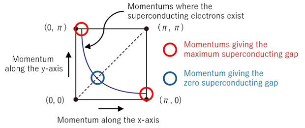
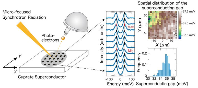
In this study, using a micro-ARPES device at the KEK Photon Factory, the researchers selectively observed electrons in the wave number direction in which the superconducting gap of a high-temperature copper oxide superconductor was maximized. By increasing the spatial resolution, the amount of data increased by several hundred times compared to conventional experiments. They also developed a method to extract and visualize the size of the superconducting gap using data science techniques.
As a result, they succeeded in visualizing, for the first time in the world, that the maximum value of the superconducting gap was nonuniform between 30 and 40 meV on the micrometer scale. Furthermore, the inhomogeneity of the superconducting gap measured by ARPES was smaller than the inhomogeneity of superconducting gap values distributed in the range of 20-70 meV reported by STM/STS.

Provided by Hiroshima University
Two energy gaps of different sizes are known to exist in high-temperature copper oxide superconductors. These gaps are the "superconducting gap" and "pseudogap." The former is a small energy gap that appears only in the superconducting state. The latter is a large energy gap that appears even at temperatures higher than the superconducting transition temperature.
Considering the size of the energy gap, it is thought that the present study reflects the spatial inhomogeneity of the superconducting gap, while using STM/STS, a mixture of the spatial inhomogeneity of the pseudogap and superconducting gap has been observed.
As a result, it can be said the spatial inhomogeneity of the superconducting gap has been captured for the first time in the world. Furthermore, the developed technique enables the visualization of spatial inhomogeneities by selecting electrons with specific wavenumbers.
This technique is expected to advance our understanding of the relationship between the "spatial inhomogeneity" and "anisotropy of wave properties" in high-temperature copper oxide superconductors and to provide a reference for elucidating the mechanism of high-temperature superconductivity exhibited by copper oxides.
The research team is currently working on increasing the intensity and micro-focusing of synchrotron radiation at the Photon Factory, HiSOR, and high-brilliance synchrotron radiation facility NanoTerasu. It is expected that this technique will develop into an even more advanced technology when integrated with high brilliance and micro-focused synchrotron radiation and will make significant contributions to the fields of materials science and applied science. In particular, it is expected to be used in numerous research and development projects as a new method to elucidate novel superconducting phenomena.
Journal Information
Publication: Science and Technology of Advanced Materials
Title: Visualization of spatial inhomogeneity in the superconducting gap using micro-ARPES
DOI: 10.1080/14686996.2024.2379238
This article has been translated by JST with permission from The Science News Ltd. (https://sci-news.co.jp/). Unauthorized reproduction of the article and photographs is prohibited.


