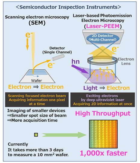
On November 7, Project Associate Professor Toshiyuki Taniuchi, Project Research Associate Hirokazu Fujiwara, Project Researcher Cedric Bareilles (currently at Hitachi High-Tech), and Project Researcher Mario Okawa of the University of Tokyo and Hitachi High-Tech announced that they are conducting joint research to commercialize a high-resolution electron microscope (Laser-PEEM: Laser-Photo Emission Electron Microscope) developed by the University of Tokyo as a semiconductor inspection device based on new principles. The two parties jointly presented the results of this research at the International Microprocesses and Nanotechnology Conference 2024 (MNC2024) held in Kyoto Prefecture from 12-15 November.

Provided by the University of Tokyo
Laser-PEEM enables faster image analyses than scanning electron microscopes (SEMs) used in the semiconductor manufacturing process. In addition, the use of a high-resolution technology developed by the University of Tokyo allows for the observation of the chemical information of materials and nondestructive observation of three-dimensional structures at the nano level. In their joint research, the two parties conducted demonstration experiments by applying the proposed high-resolution Laser-PEEM to the semiconductor field to commercialize an inspection system to find device defects and confirmed its usefulness.
The first result is the realization of rapid nanoscale observations. Laser-PEEM irradiates the entire observation object with a laser rather than an electron beam and obtains an observed image by capturing electrons emitted from the object with a camera, yielding wide-area, high-resolution data all at once. The joint research demonstrates that the inspection process can be performed in a considerably shorter time compared to SEM, which uses scanning electron beams.
The second result is the application of the new microscope in the inspection of defects in a circuit pattern formed via semiconductor lithography. Circuit pattern forming involves three main processes: resist coating, exposure, and development. The resist exposed to light during the exposure process changes its material properties so that it can be removed in the subsequent development process. However, only slight changes occur on the material surface, and there is almost no uneven pattern.
Therefore, to inspect the exposed circuit pattern for defects, it is necessary to go through the following development process to form an uneven pattern that can be observed using SEM. By contrast, Laser-PEEM allows to visualize material differences (latent image patterns) as well as unevenness and thus has the potential to perform inspection during the exposure process prior to the development process.
In this joint research, Laser-PEEM was used for the first time in the world to observe latent image patterns during the exposure process, demonstrating that observations can be made with a high resolution and a high throughput. This latent image pattern observation is not possible using conventional methods, and by making it possible, the new method is expected to create a new inspection market that has never existed before. When the inspection throughput of conventional post-development pattern inspection performed via SEM was evaluated using Laser-PEEM, it was found to be 10,000 times faster than the electron microscope observation, decreasing the inspection process duration in existing semiconductor manufacturing.
The third result is the realization of the nondestructive observation of nanostructures. High-resolution Laser-PEEM can detect depths of approximately 10-100 nm.
The joint research demonstrated that it is now possible to "see through" defects and their causes in wafers in a nondestructive manner. Previously, wafers had to be processed and observed to analyze the causes of defects, but this can now be done in a nondestructive manner, which helps reduce the amount of work required for processing and enables more accurate analyses.
Hitachi High-Tech will continue this research in collaboration with the University of Tokyo to gather timely information regarding the needs of semiconductor manufacturers who use this technology and to commercialize this technology as a product that will solve issues in the manufacturing and shipping processes. In addition, as Laser-PEEM can provide more information regarding an observed object than electron microscopes. It is expected to contribute not only to the semiconductor industry but also to various other industrial fields and fundamental science in the future. The two parties will continue collaborative research on the application of this technology to solve various social issues.
This article has been translated by JST with permission from The Science News Ltd. (https://sci-news.co.jp/). Unauthorized reproduction of the article and photographs is prohibited.


