
Efficient hydrogen production is necessary for the realization of a hydrogen society. Transition-metal dichalcogenides (TMDs), including molybdenum disulfide (MoS2), are attracting attention as catalysts for electrochemically generating hydrogen from water, instead of the more expensive platinum. Meanwhile, in the semiconductor field, TMDs are emerging as strong candidates for next-generation semiconductors because they exhibit excellent electrical properties with only three atoms, while the properties of silicon are compromised when it is thinned to the atomic level.
A research group including Doctoral Student Ma Zongpeng, Associate Professor Pablo Solís-Fernández, and Distinguished Professor Hiroki Ago of the Interdisciplinary Graduate School of Engineering Sciences at Kyushu University; Professor Yasufumi Takahashi of the Graduate School of Engineering at Nagoya University; Associate Professor Toshiaki Kato of the Advanced Institute for Study of Materials Science at Tohoku University; Professor Susumu Okada of the Institute of Pure and Applied Sciences at the University of Tsukuba; Professor Kazutomo Suenaga of the Institute of Scientific and Industrial Research at Osaka University; Senior Researcher Yung-Chang Lin of the National Institute of Advanced Industrial Science and Technology; Professor Kazunari Matsuda of the Institute of Advanced Energy at Kyoto University; and Associate Professor Masahiro Hara of the Faculty of Advanced Science and Technology at Kumamoto University, developed a new method to grow high-density MoS2 nanoribbons on a substrate by chemical vapor deposition (CVD). Through nanoscale electrochemical measurements, the research group found that the edges of the nanoribbons exhibit nearly 100 times higher catalytic activity than the center. Furthermore, it was found that these nanoribbons exhibit excellent electrical properties as semiconductor materials. The results were published in Science Advances.
Provided by Kyushu University.
Ago said, "The MoS2 nanoribbons prepared in this research are expected to be used as catalysts due to their extremely high edge ratio and show promise as next-generation semiconductor materials for use in 2030s. In the future, we will continue to pursue even more unique and original research, including the development of higher integration of TMDs."
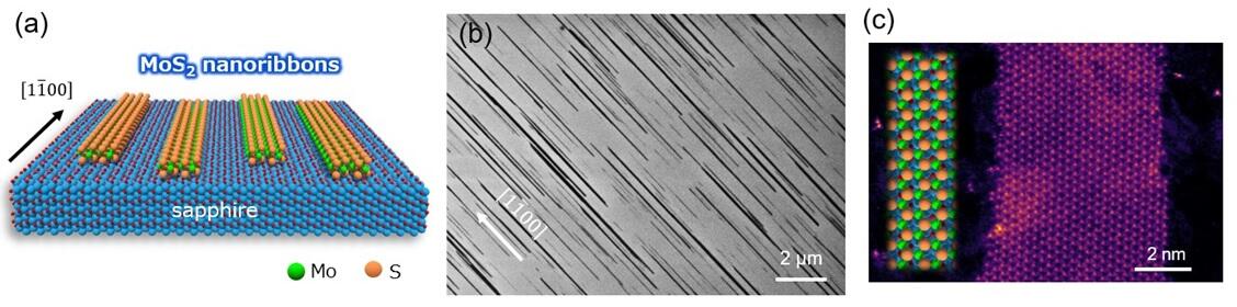
The research group succeeded in synthesizing high-density MoS2 nanoribbons aligned in one direction using an a-face sapphire substrate with an anisotropic surface atomic arrangement wherein atoms were aligned differently depending on their orientation by investigating the synthesis conditions in detail. Specifically, MoS2 nanoribbons were synthesized by CVD on a sapphire substrate at 1100°C under argon gas flow using molybdenum oxide (MoO3) and sulfur (S) as raw materials.
Scanning electron microscopy (SEM), nanoribbon height measurements, and spectroscopic measurements confirmed that the nanoribbons were made of single-layer MoS2 (thickness equal to that of three bonded atoms (S-Mo-S)). The unidirectional growth was attributed to the anisotropic surface atomic arrangement on the sapphire substrate. Although reports on MoS2-nanoribbon synthesis have been published in the past, the synthesizing process of nanoribbons was inefficient as atomic steps were first formed on a special substrate, and nanoribbons were in turn grown along the steps. Their edge structure was greatly disordered, like the edge of a saw. In addition, there were many defects in the solution synthesis process. Scanning transmission electron microscopy (STEM) observations confirmed that the nanoribbons prepared in the study had a single-crystal MoS2 structure with almost no defects. Further, the edges were found to be comparatively smooth.
These oriented MoS2 nanoribbons were transferred onto a conductive graphite substrate and their electrochemical catalytic activity was measured. The researchers attempted to visualize the catalytically active sites for the hydrogen evolution reaction (HER) using scanning electrochemical cell microscopy (SECCM) with a very thin glass tube (pipette) filled with an electrolyte at the tip. The results showed that the catalytic activity was higher at the edges of the nanoribbons.
Detailed analysis of the current values showed that the catalytic activity was nearly 100 times higher at the edges than at the center. Furthermore, the edge/area ratio was large for thin nanoribbons, indicating high HER activity per unit area. In addition, it was found that the edges exhibited the lowest voltage at which the HER occurred. This indicated that the nanoribbons with a high percentage of edges were suitable for hydrogen generation.
To investigate the semiconductor properties of the nanoribbons, ultrafine devices were fabricated using the nanoribbons and their electrical properties were evaluated after transferring the nanoribbons from the a-face sapphire substrate to a silicon substrate.
The result showed that a transistor operation was achieved using a thin nanoribbon with a width of 110 nm. Further, electron mobility values comparable to or higher than those of regular MoS2 sheets were obtained. It is difficult to fabricate such thin nanoribbon structures by lithography and etching. Even if thin nanoribbons can be fabricated by these methods, the edges would be extremely disordered. Thus, the MoS2 nanoribbons growing in a self-aligned manner that are prepared in the study showed excellent potential as ultrathin and fine channels.
When the MoS2-nanoribbon-based device was cooled to cryogenic temperatures and measured, the nanoribbons behaved as multiple quantum dots--showing a property called Coulomb diamond--confirming their low dimensionality and high crystallinity. The nanoribbons are also promising as channels for next-generation semiconductors. In addition to MoS2, the research group succeeded in preparing tungsten disulfide (WS2) nanoribbons and synthesized heterostructured nanoribbons with WS2 around MoS2.
Journal Information
Publication: Science Advances
Title: Lattice-guided growth of dense arrays of aligned transition metal dichalcogenide nanoribbons with high catalytic reactivity
DOI: 10.1126/sciadv.adr8046
This article has been translated by JST with permission from The Science News Ltd. (https://sci-news.co.jp/). Unauthorized reproduction of the article and photographs is prohibited.