
Oxides, such as vanadium oxide, have a mechanism different from those of conventional semiconductor materials and can perform large-scale switching operations. They are considered promising materials for use on a nanoscale even after achieving the maximum miniaturization of silicon semiconductors. However, the ultrathin film deposition of such oxides is possible only on special and expensive materials with identical crystal structures to these oxides, rendering developing such materials for general applications a challenge.
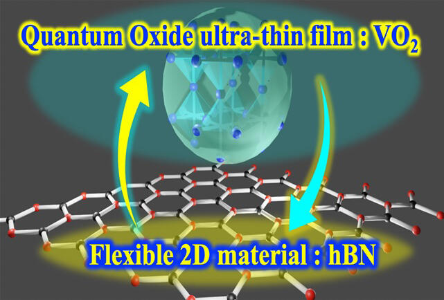
A research group including Doctoral Student Boyuan Yu and Professor Hidekazu Tanaka of SANKEN at Osaka University, and Dr. Kenji Watanabe and Dr. Takashi Taniguchi of the National Institute for Materials Science (NIMS) used pulsed laser deposition to grow a thin film of vanadium dioxide (VO2) crystals on hexagonal boron nitride (hBN), a 2D material. The research group demonstrated for the first time in the world that performance did not deteriorate even at a small thickness and that even an ultrathin film that was about 10-nm thick exhibited excellent switching characteristics. This result will enable oxide quantum materials to be freely converted to the nanoscale regime, and their flexible nature allows for their attachment to numerous materials, improving the ease of sensor and device fabrication. This result will lead to the development of new applications in the semiconductor industry. The results have been published in Applied Physics Express.
Provided by Osaka University
hBN, provided by the NIMS group, is a 2D material comprising a hexagonal lattice similar to graphene, which is famous for its ability to be peeled off into single-atom layer sheets. Only very weak bonding forces, called van der Waals forces, are acting on its atomically flat sheet-like surface, making it very soft. This characteristic is very different from the strong covalent and ionic bonds of oxide materials, which are also used as ceramics.
The research group hypothesized that no undue strain would be introduced on the surface of this soft hBN, even when different materials were combined, and that strain at the interface would be reduced and oxide materials would grow. Using pulsed laser deposition, they fabricated thin films of various thicknesses and evaluated their switching characteristics. The researchers succeeded in growing ultrathin VO2 films that did not degrade when the thickness was decreased and showed excellent characteristics even at a thickness of 10 nm.
Layered structures between soft organic materials are well known. However, the direct layer-by-layer growth of rigid, inorganic strongly correlated quantum materials on two-dimensional soft materials, as in this case, may open up new interface physics phenomena.
Tanaka said, "By combining materials with different chemical properties, we expect to increase the degree of freedom in the material design and develop new functions that has remained impossible before. Combinations of similar inorganic materials can be interesting, but if bonds are too strong, the combinations of materials that can be developed are limited. 2D materials have very weak bonds and do not interact much. We thought that by taking advantage of this characteristic, they could be grown even with different crystal structures; hence, we proceeded with this research. In the future, we want to clarify the phenomenon occurring at the interface, which remains unclear, and combine quantum functional oxide materials with 2D materials to develop properties that can only be achieved by doing so."
Journal Information
Publication: Applied Physics Express
Title: Strain-free thin film growth of vanadium dioxide deposited on 2D atomic layered material of hexagonal boron nitride investigated by their thickness dependence of insulator-metal transition behavior
DOI: 10.35848/1882-0786/adaf09
This article has been translated by JST with permission from The Science News Ltd. (https://sci-news.co.jp/). Unauthorized reproduction of the article and photographs is prohibited.