
In recent years, the fabrication of sheet-like materials of only a few atoms thick has become possible, attracting significant attention. There are many types of such sheets, exhibiting various physical properties, including metallic, magnetic, and superconducting characteristics. When multiple sheets are stacked, new properties emerge. Additionally, dramatic changes in physical properties can occur when stacked sheets are twisted relative to each other. However, the impact of stacking and twisting on electronic states, especially on superconductivity, has been difficult to investigate experimentally and was largely unknown until now.
The Emergent Phenomena Measurement Research Team from the Center for Emergent Matter Science at RIKEN, including Research Scientist Masahiro Naritsuka, Senior Research Scientist Tadashi Machida, and Team Leader Tetsuo Hanaguri, formed a joint research team with Graduate Student Shun Asano and Professor Youichi Yanase from the Graduate School of Science at Kyoto University, and discovered that the properties of superconductivity can be controlled by stacking atomic-level thin superconducting sheets with other atomic sheets and applying a twist to their crystal axes. Their findings were published in Nature Physics.
Provided by RIKEN
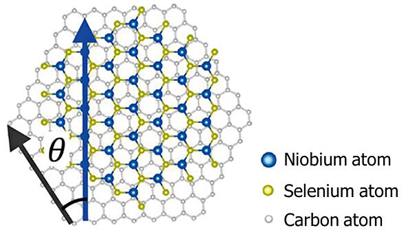
The joint research team stacked the atomic sheet superconductor NbSe2 (niobium diselenide) with graphene, known as a carbon atomic sheet, and twisted them. They then used scanning tunneling microscopy/spectroscopy (STM/STS), which can map the spatial distribution of electrons with various energies, to examine in detail the effect of twisting on the superconducting state.
At RIKEN, researchers have independently developed a scanning tunneling microscope that operates in ultra-low temperature environments, achieving temperatures below 0.09 K, the world's lowest temperature for a device capable of stable STM/STS. This is sufficiently lower than the critical temperature of 1-2 K for the atomic sheet superconductor NbSe2, allowing for the investigation of intrinsic properties of the superconducting state. The joint research team adopted silicon carbide (SiC), a compound of silicon and carbon, as a substrate for the stacked structure. They created graphene on the substrate surface by heating SiC in a vacuum to desorb the silicon. Next, using molecular beam epitaxy (a high-quality thin film fabrication method) in the same vacuum chamber, they grew a monolayer atomic sheet of NbSe2 on the graphene. By precisely controlling the growth temperature, they were able to create a "twisted stack" where the crystal axes of graphene and NbSe2 were misaligned.
When transporting samples between devices, exposing the sample surface to the atmosphere can lead to contamination due to reactions with oxygen and other air components. To prevent this, they used an "ultra-high vacuum suitcase" that maintains an ultra-high vacuum environment, allowing the samples to be transferred without any exposure to air. Various such technological developments made this experiment possible for the first time. Superconductivity arises when electrons form pairs (Cooper pairs). Since energy is required to break Cooper pairs and return them to normal electrons, electrons cannot exist in low-energy regions in the superconducting state (these energy regions are the superconducting gap). Since STM/STS is a method for observing normal electrons, nothing should be observed when experiments are conducted at energies within the superconducting gap. When examining the electronic state distribution of NbSe2 and graphene stacked structures with various twist angles, the team found no electronic states within the superconducting gap when the twist angle was 0 degrees. However, in stacked structures with twist angles of 24 and 28 degrees, a small number of electronic states appeared within the superconducting gap energy, showing a ripple-like spatial pattern.
Analysis using Fourier transform to determine what wavelength components were included in the observed spatial patterns and in which directions they appeared revealed that wave components appeared in a twisted direction that was misaligned from both the crystal axes of NbSe2 and the crystal axes of graphene.
The observed wave-like spatial patterns reflect the quantum-mechanical wave nature of electrons. In crystals, the wavelength and direction of propagation of electrons are restricted due to the influence of periodically arranged atomic nuclei. These wavelengths and directions of propagation depend on the arrangement of atomic nuclei and thus differ for each material. Therefore, the electrons in NbSe2 and graphene have different wavelengths and directions of propagation.
However, analysis of theoretical calculations of the electronic states of NbSe2 and graphene revealed that there are twist angles at which some electrons from stacks of each material have the same wavelength and direction of propagation. The wavelength and direction of propagation in the twisted stack obtained experimentally perfectly matched those calculated theoretically. These results suggest that electrons from graphene, which is not superconducting, influence the superconductivity of NbSe2, selectively suppressing the formation of Cooper pairs via electrons with matching wavelengths and directions of propagation. This provides a new method for controlling superconductivity by specifying the wavelength and direction of propagation of electrons.
The insights gained from this study can be applied beyond stacked structures of NbSe2 and graphene. Using atomic sheets with other functions, such as magnetic materials, may lead to unique devices where only electrons with specific wavelengths and directions of propagation exhibit magnetism. Furthermore, by further developing sample fabrication techniques and increasing the number of twisted layers to realize complex and advanced stacked structures, it is expected that previously unknown novel superconducting phenomena and topological quantum phenomena may be discovered.
Journal Information
Publication: Nature Physics
Title: Superconductivity controlled by twist angle in monolayer NbSe2 on graphene
DOI: 10.1038/s41567-025-02828-6
This article has been translated by JST with permission from The Science News Ltd. (https://sci-news.co.jp/). Unauthorized reproduction of the article and photographs is prohibited.