
A collaborative research group including Graduate Students Kenji Oki and Shinnosuke Ueda, and Professor Kohei Hamaya from the Graduate School of Engineering Science at University of Osaka, Lecturer Takamasa Usami from the Institute for Open and Transdisciplinary Research Initiatives at University of Osaka, Professor Keisuke Yamamoto from the Research and Education Institute for Semiconductors and Informatics at Kumamoto University, and Professor Kentaro Sawano from the Advanced Research Laboratories at Tokyo City University has succeeded in observing spin conduction at room temperature for the first time in the world in a device structure with a semiconductor 𝑝-𝑛 junction. Their findings were published as a Letter in Physical Review Applied.
Provided by the University of Osaka
With the proliferation of AI, power consumption in large-scale data centers continues to increase significantly. Therefore, development of next-generation semiconductor spintronics devices that combine low-power computing functions with non-volatile memory capabilities is advancing. To realize non-volatile memory functionality, it is essential to demonstrate spin conduction, where electrons conduct through semiconductors while maintaining their magnetic properties (spin).
The research group had previously developed a unique structure that directly bonds, at high quality, semiconductor germanium (Ge) with high-performance spintronics magnetic materials (ferromagnetic Heusler alloys), demonstrating room-temperature spin conduction. However, since typical semiconductor devices contain 𝑝-𝑛 junctions that control current on/off switching, it is necessary to observe room-temperature spin conduction in device structures containing these 𝑝-𝑛 junctions.
Previous research has only utilized III-V ferromagnetic semiconductors that operate solely at extremely low temperatures. It was unclear how 𝑝-𝑛 junctions would affect the room-temperature operation of spin devices.
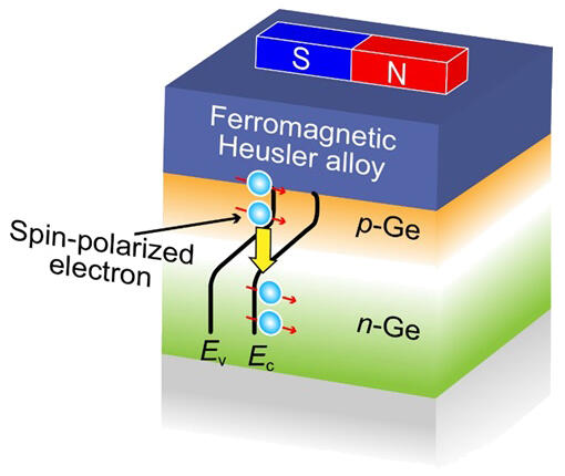
The research group conceived a new approach of applying tunnel FET (TFET) technology, which uses quantum mechanical band-to-band tunneling (BTBT) conduction for current modulation, to semiconductor spintronics devices. As a first step toward realizing spin TFETs, a new type of semiconductor spintronics device, the research successfully incorporated 𝑝-𝑛 junctions into structures that directly bond, at high quality, semiconductor Ge with ferromagnetic Heusler alloys, and succeeded in observing room-temperature spin conduction via BTBT conduction in 𝑝-𝑛 junctions. This represents an important step toward realizing spin TFETs.
Hamaya commented: "This achievement is not the outcome of research that chased after 'cutting-edge trends,' but rather research that overcame challenges that have existed for over 10 years using our laboratory's technology. I believe this is the result of the fusion of science and technology that we have steadily accumulated for over 10 years now beginning to bear fruit. I am grateful that Physical Review Applied has chosen to publish even this kind of research as a Letter (rapid communication)."
Journal Information
Publication: Physical Review Applied
Title: Room-temperature spin transport through band-to-band tunneling at semiconductor 𝑝-𝑛 junctions
DOI: 10.1103/PhysRevApplied.23.L051005
This article has been translated by JST with permission from The Science News Ltd. (https://sci-news.co.jp/). Unauthorized reproduction of the article and photographs is prohibited.