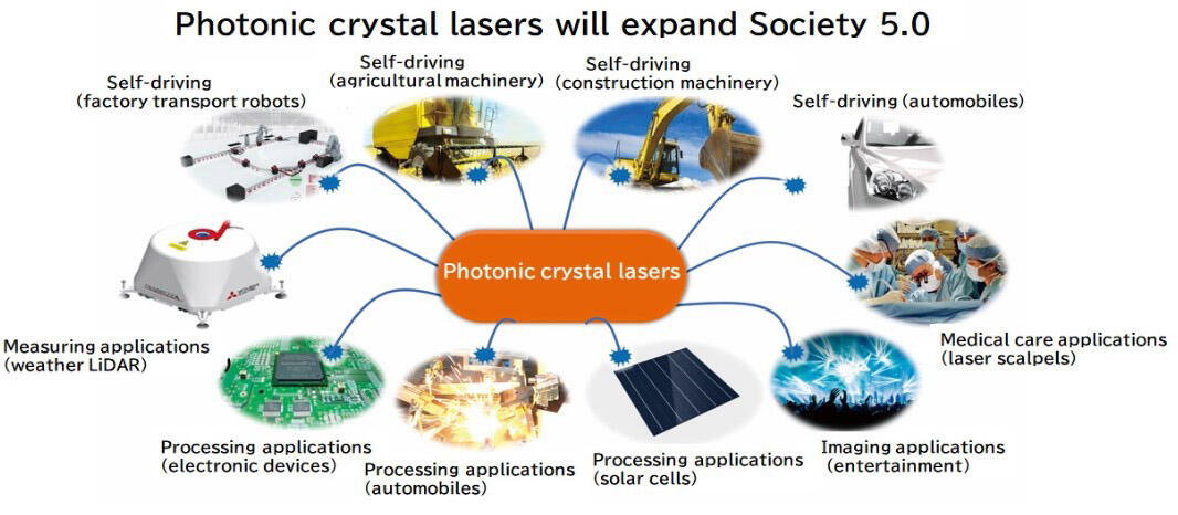
"Photonic crystals" freely control light. In recent years, significant progress has been made with photonic crystal lasers as one of the enabling technologies for 'Society 5.0', including smart mobility. We look back at the course taken by Professor Susumu Noda of the Graduate School of Engineering, Kyoto University, who has been engaged in this research for the last 20 years.
Self-driving cars draw close to being put into practical use
Enhancing sensor performance remains a challenge
The development of autonomous mobile robots and self-driving cars is moving forward, and they are now at the stage of being within reach of practical application. Nevertheless, several challenges remain in order to make them practically viable, and one such challenge is enhancing the performance of Light Detection and Ranging, or LiDAR.
LiDAR sensors are one type of remote sensor. They are a system that measures the distance to an object by targeting the object with a laser beam and measuring the time it takes for the reflected beam to return. Autonomous mobile robots and self-driving cars move while constantly identifying the circumstances of their surroundings, and for them, LiDAR systems perform the role of the "eyes." If the performance of those "eyes" improves, it will become possible for the robots and cars to move more safely and smoothly. In light of that, the race to develop LiDAR systems has been picking up pace in recent years.
Up to now, semiconductor lasers have been used as LiDAR systems' sources of light, but despite them being small, cheap and easy to handle, at high output powers , the beam of laser light diverges and their performance declines. Consequently, strategies such as collimating the beam by combining multiple lenses have been employed, but the resulting increases in the size and cost of the systems have proven problematic.
In June 2020, Professor Susumu Noda of the Graduate School of Engineering, Kyoto University, in partnership with Hokuyo Automatic Co., Ltd. (Osaka City, Osaka Prefecture), developed a high-performance LiDAR system that uses a "photonic crystal laser." Professor Noda is the leading authority on photonic crystals, and over a period of around 20 years, he has pursued research and development and built the foundations of a new field of science technology known as "photonic crystal engineering." The photonic crystal laser that Professor Noda has announced could also be described as one culmination of those efforts.
Controlling light with periodic structure; same principle as in the natural world
Photonic crystals are artificial crystals (Fig. 1) in which materials with different refractive indices are arranged periodically at intervals of several hundred nanometers (one nanometer is one-billionth of a meter), which is comparable to the wavelength of light. In the same way that semiconductors precisely control the behavior of electrons in the field of electronics, photonic crystals are notable for being able to freely control the behavior of light.
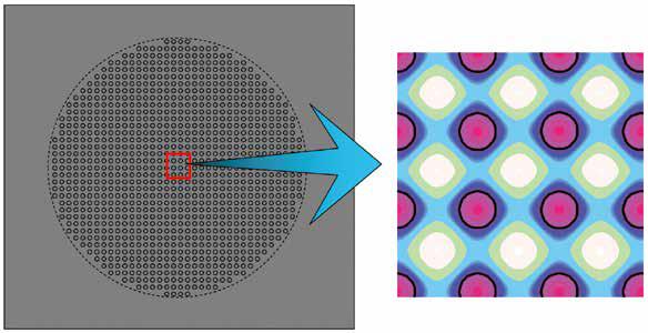
An electromagnetic field distribution (the magnetic field component in a perpendicular direction to the page) that is controlled by photonic crystals. The pink and white-colored areas show that the respective magnetic fields are in opposite directions (right).
Photonic crystals possess a periodic structure with intervals that are comparable to the wavelength of light. Within them, a "photonic band gap phenomenon" appears, whereby light of a certain wavelength range will not pass through them. A large number of examples based on the same principle are found in the natural world. The surfaces of morpho butterflies, jewel beetles and opals also have fine periodic structures, and these exhibit unique brilliance, which is referred to as structural coloration.
For periodically arranging materials with different refractive indices, a method of opening holes in the materials can be used. It is possible to control the behavior of light by specifically designing the intervals between the holes, and their position, size and shape. "As a base material for photonic crystals, currently we are employing semiconductors such as gallium arsenide. That is because such semiconductor materials are extremely useful for a variety of devices," Professor Noda explains.
High-power and narrow-divergence laser beam realized by adopting a double lattice
In 1999, Professor Noda focused on the fact that at band edges, which appear at the edge of the photonic band gap, a state of resonance across a large area is formed, and he arrived at the idea of using this state of resonance as a semiconductor laser's resonator. He actually realized a photonic crystal laser by integrating photonic crystals into semiconductor lasers and utilizing this state of resonance. In doing so, as expected, applaudable oscillation was obtained across a large area, and furthermore, the laser beam was emitted in a direction perpendicular to the surface with a very small divergence. Ever since, Professor Noda has been working diligently to clarify the physics of photonic crystal lasers, as well as to enhance their unique properties. Those efforts have contributed to making LiDAR systems smaller, lighter and more inexpensive, as well as boosting their output power and stability. These advances are now generating considerable expectations.
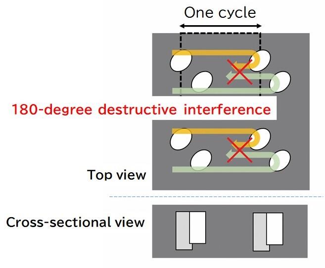
Among all these efforts, a particularly important breakthrough was making the periodic structure of the photonic crystals a double lattice. Conventionally, there had been one hole per lattice point, but Professor Noda made this into two holes and changed their respective heights (Fig. 2). "The idea of the double lattice itself was something I had hit upon quite some time ago, but at the time, it was still not possible to carry out the theoretical calculations, and neither did the technology exist to accurately create photonic crystals this fine," Professor Noda recalls. With these double lattice photonic crystals, interference occurs in which the light waves diffracted on each of the lattices cancel each other out and the light distribution spreads out in the plane of the photonic crystal . Professor Noda found that as a result, it is possible to operate them in a single fundamental mode and produce a high-quality laser beam. This led to the development of a high-beam-quality laser with a high, 10-watt-level output power. This laser had a diameter of 500 micrometers, which is more than 10,000 times the area of conventional semiconductor lasers.
In addition, by changing the combination of the two holes, Professor Noda also succeeded in aligning their heights and enabled the manufacturing process to be shortened. He also strove to effectively utilize the downward radiated light to enhance efficiency (Fig. 3). These can quite literally be described as outcomes that were obtained through the accumulation of microfabrication technologies, backed by theories arising from meticulous calculations.
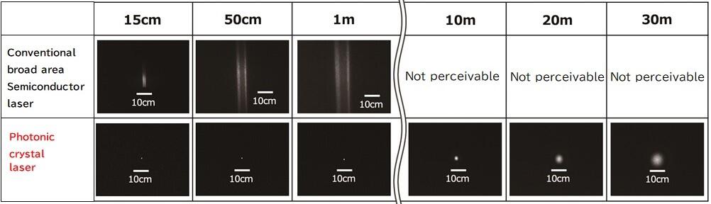
When the photonic crystal laser developed in this fashion was actually compared with a conventional semiconductor laser, the laser beam produced using a semiconductor laser not shaped with lenses ended up gradually spreading, but the laser beam produced with the photonic crystal laser reached a point approximately 30 meters away with almost no spread, even without lenses (Fig. 4). "It was demonstrated in experiments that the performance photonic crystal lasers possess is sufficient to allow them to be applied to self-driving robots. As a result, it has become possible to make smaller, lighter and more inexpensive LiDAR systems that boast high output power and are stable, and thus overcome the majority of the problems associated with conventional semiconductor lasers," Professor Noda explains proudly.
High-precision detection of objects achieved with beam scanning in two dimensions
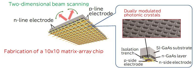
Subsequently, Professor Noda also succeeded in developing a "dually modulated photonic crystal laser chip" capable of controlling beam emissions in various directions electrically. Furthermore, in partnership with Brookman Technology, Inc. (Hamamatsu City, Shizuoka Prefecture), a venture company that originated at Shizuoka University, Professor Noda used this laser chip to develop a new non-mechanical LiDAR system that uses the flash method and the beam scanning method in combination.
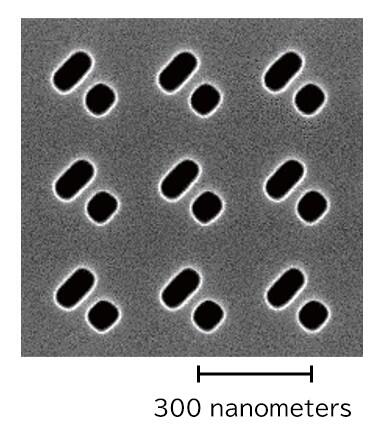
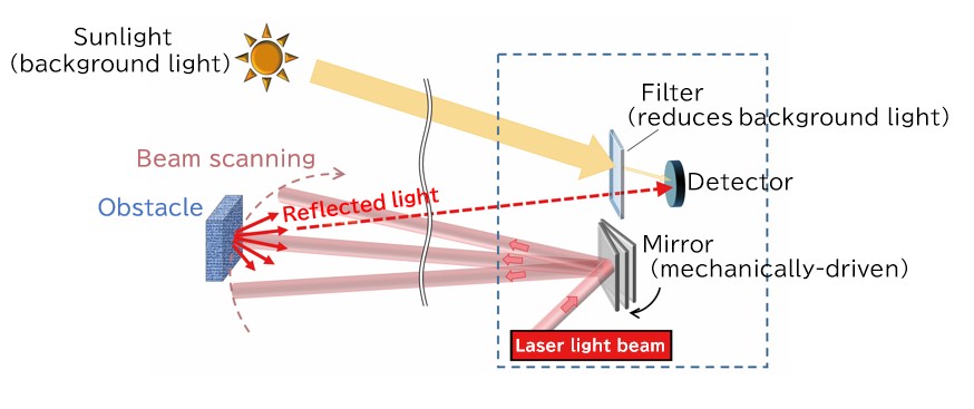
In conventional LiDAR systems, the angle of mirrors used to reflect the laser beams is adjusted to make it possible to scan broad areas (Fig. 5). By comparison, Professor Noda, who had already succeeded in developing a technology for beam scanning in a one-dimensional direction, took that technology one step further and made it possible for the laser beam to be allocated to various angles electrically, without installing mirrors, as a result of beam scanning in two dimensions. In basic photonic crystals, holes of the same shape and size are arranged at regular intervals, but in the dually modulated photonic crystals, both the position and size of the holes are changed, which makes it possible to radiate laser beams in arbitrary directions (Fig. 6).
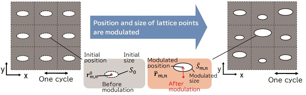
Developing this technology also involved hardships. "Initially, I had thought I would only have to change the position of the holes, but for some reason, the output power did not increase. In the course of repeatedly carrying out experiments, I noticed that, as a result of the electric fields canceling each other out, light is not emitted," Professor Noda recalls. By also changing the size of the holes to disrupt this mutual cancelation, he realized a high-output-power, high-quality beam.
Professor Noda then integrated one hundred laser elements, each with its own dually modulated photonic crystal, onto a single chip in the configuration of a 10x10 matrix array (Fig.7). With this chip, by designating specific rows and columns in the 10x10 matrix and passing electricity through them, a laser beam can be emitted only from the laser element in that location. Since the direction of the laser beam that is emitted by each laser element differs, controlling the laser elements electrically gives rise to a mechanism for using laser beams for two-dimensional scanning. As a result of this, it became possible to emit laser beams of several watts in several separate directions, simultaneously.
Furthermore, Professor Noda also found that simply by increasing the chip area by four times, the number of beams emitted could be increased to 90,000, or 900 times the current number, which will make it possible to detect objects in a surrounding area with higher accuracy. Noting one advantage of the technology, Professor Noda points out that "In particular, black objects have been difficult to measure with LiDAR systems that only use the conventional flash method, but by using the flash method in combination with a beam scanning method that utilizes these chips, it becomes possible to concentrate the laser beam onto such objects and measure their distance."
Shining leadership: 20 years working with JST
Professor Noda began researching and developing photonic crystals in the 1990s, and for approximately 20 years since 2000, he has been pursuing research in JST's programs.
Professor Noda's achievements over that period are too numerous to mention. He was selected by CREST in 2000 and 2005 and engaged in generating and controlling light using photonic crystals--a field still in its infancy at that time--and built the base for that technology. Amid that, Professor Noda substantially advanced photonic crystal laser technology. Furthermore, from 2011, when there was a push to promote the use of natural energies in the immediate aftermath of the Great East Japan Earthquake, in contrast to photonic crystal lasers, he capitalized on the periodic structure of photonic crystals to instead make it possible to absorb a broad range of wavelengths, and in doing so successfully increased the energy conversion efficiency of silicon solar cells.
Additionally, in his time at ACCEL from 2013, Professor Noda collaborated with companies such as Mitsubishi Electric Corporation. (Chiyoda Ward, Tokyo), Rohm Co., Ltd. (Kyoto City, Kyoto Prefecture) and Hamamatsu Photonics K.K. (Hamamatsu City, Shizuoka Prefecture), and engaged in research and development aimed at putting photonic crystal lasers into practical use. It was around this time that Professor Noda came up with his concept for a modulated photonic crystal laser. "At that time, research and development on self-driving cars was beginning to gain momentum, which led me to engage in developing two-dimension beam scanning technology using modulated photonic crystal lasers at CREST, where I am working. Furthermore, I was also fortunate enough to be selected for a cross-ministerial SIP Project, which prepared the framework for forging powerfully ahead with social implementation in conjunction with CREST."
When discussing these achievements, Professor Noda's leadership cannot be overlooked either. "When pursuing research, both in the laboratory and in project teams, I held robust meetings, and moved forward while respecting each member's thoughts and consolidating our direction as a team. As a result of individuals with different specialties interacting and pooling their knowledge, it was possible to make '1+1=3'," Professor Noda explains. With this policy, he also took into account the training of young researchers who will carry research into the future. Furthermore, his attentive communication with the companies that are involved in developing fabrication equipment is also contributing to the enhancement of technical capabilities.
Looking ahead, Professor Noda says to begin with, he will aim to work with companies to put LiDAR systems that are equipped with photonic crystal lasers into practical use as quickly as possible. Additionally, Professor Noda is also planning to realize continuous-wave operation of lasers and enhanced brightness, and develop ultra-small processing lasers to replace conventional carbon dioxide gas lasers and other lasers. "It is my dream that all lasers will be replaced by photonic crystal lasers in the future," Professor Noda explains. He will continue to work enthusiastically with his colleagues, aiming for the day when his achievements form a base technology supporting the next generation society (Society 5.0).
Professor, Graduate School of Engineering, Kyoto University
Research Director of CREST since 2000 (2000-2005, 2005-2010, 2011-2016, 2017-present), Research Director of ACCEL, 2013-2018