To meet the needs of a diversifying society, there is an increasing demand for highly versatile semiconductors that can be rewritten by developers. In response to these demands, NanoBridge Semiconductor, Inc. (NBS) (Tsukuba, Ibaraki Prefecture) is addressing the challenge of the mass production of semiconductors that use metal atoms in the switch components of circuits. Innovative products that are compact, reduce power consumption, and radiation-resistant will accelerate global ICT research and development.
A focus on FPGA IoT and AI utilization with a high flexibility
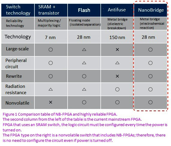
With the development of the Internet of Things (IoT), we are entering an era in which desired information can be obtained instantly via a terminal and operating a device remotely. This accessibility is supported by the increasing capacity and sophistication of integrated circuits (ICs), which instantly process a large amount of information. ICs those are receiving particular attention currently are "field-programmable gate arrays" (FPGAs) (Fig. 1). FPGAs can be reconfigured by users as often as desired, and there is no need to re-fabricate them in case of specification changes or to purchase expensive dedicated products. The development risk is also reduced, and the turn-around time can be shortened. Currently, FPGAs are mainly used in high-definition cameras for broadcasting stations and in base stations for mobile phones; however, their potential as devices that support infrastructure is increasing.
On the other hand, FPGAs require a power supply to store circuit information and have large chip sizes. Therefore, NBS has developed an FPGA that uses "atomic switch " technology, which utilizes migration of metal atoms. "We have achieved FPGAs whose size and power consumption are lower than those of FPGAs with similar processing performance, " says NBS President, Tadahiko Sugibayashi.
Power efficiency improved approximately ten times using atomic switch
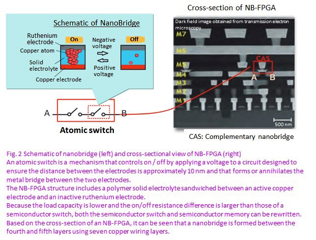
Dr. Masakazu Aono studied atomic switch technology in a CREST project and proved its feasibility in 2001. An atomic switch is controlled by the formation or annihilation of a nanometer-sized bridge called a "NanoBridge " made of metal between a solid electrolyte and the metal electrode (Fig. 2). "It all started for the development of this technology when I was asked to integrate atomic switches., " recalls NBS Chief Technology Officer, Toshitsugu Sakamoto. When the atomic switch technology was adopted by Solution Oriented Research of Science and Technology (SORST) in 2000 and practical research began, application of an atomic switch was considered for a nonvolatile memory element that can hold information without requiring power supply was considered. However, with the aims of reducing the size and improving the reliability of FPGAs, a decision was taken to implement an atomic switch inside an FPGA. In 2011, Developing a prototype of a NanoBridge-FPPA (NB-FPGA) was succeeded by using a metal atom mobile switch using copper, which was already being utilized for semiconductor wiring.
Another CREST project that started in 2014 aimed to replace the "static random-access memory" (SRAM) of semiconductors, which requires power to hold memory, with atomic switches. Consequently, a size reduction to approximately one-third of that of conventional FPGAs was achieved, and the power efficiency improved approximately ten times. By replacing approximately a quarter of the SRAM with atomic switches, the quality was stabilized and samples could be shipped. "Basic research that began in the 1990s has finally matured through a number of Japan Science and Technology Agency projects," says Sakamoto, speaking with deep emotion. He is currently working on a product in which everything used in SRAM-type FPGA is replaced by atomic switches. "We have succeeded in fabricating a prototype, and therefore, are developing the technology for mass production," says Sakamoto, considering the next problem.
High performance, but demand is sluggish A way forward for demonstration experiments in space.
Although product development was smooth and sample shipments started in 2017, the demand was sluggish. First, discussions with relevant people introduced them to the "Innovative Satellite Technology Demonstration Program" of the Japan Aerospace Exploration Agency. Traditional FPGAs have not been utilized in space owing to unpredictable errors under radiation effects. "NB-FPGA is characterized by radiation resistance. Because it uses a metal, it is not easily affected by radiation, and the error rate of the element itself is significantly reduced. Even in case of an unexpected scenario occurring after launch, its circuit can be changed. I applied because I thought it was suitable for use in space," says Sugibayashi. NBS built the NB-FPGA into a camera and seeking an opportunity by conducting demonstration experiments in outer space. It is expected that the performance of NB-FPGA will be demonstrated in artificial satellites that require high performance and that conventional FPGAs will be replaced with the NB-FPGAs.
Collaborating with the right people in the right place to best utilize excellent technology
When it was finally put into practical use, the semiconductor division of NEC, which was enrolled at that time, was closed. "I thought that if we abandon the practical use of NB-FPGAs, this excellent technology would be forgotten. Therefore, we established NBS and started a business in 2019 to utilize it in society," said NBS Executive Vice President, Munehiro Tada, looking back at that time. At NEC, Sugibayashi, Dr. Sakamoto, and Dr. Tada oversaw commercialization, technology development, and development and manufacturing, respectively; and then, NBS also acquired the system as it is.
Fortunately, they could collaborate with the right people in the right places; however, Dr. Sugibayashi emphasizes that high R&D and financing capabilities are also important for the success of a venture. "Simultaneously, as we seek the next business opportunity in R&D, we must raise as much funding as we need and when we need it, to ensure we don't exhaust our financial resources." It is also necessary to make calm management decisions to sell what can be sold, even if the performance levels drop by a step, based on the needs of the market. "It may be important to vocalize the problems you are encountering. More people than I expected helped and supported us," adds Sakamoto. The barriers for the introduction of NB-FPGAs have been lowered by the adoption of a manufacturing method that can use conventional semiconductor manufacturing lines. "The mask technology for integrating the atomic switch on semiconductor chips is the same as conventional technology. The challenge is how to create an electrolyte layer and other components, which are not used in conventional semiconductors, using existing equipment," Tada says.
Currently, an NB-FPGA is manufactured in the standard 65-nanometer technology in cooperation with domestic semiconductor manufacturers; however, it needs to be miniaturized to 28 nm for widespread use in the communication field. "Because Japan does not have equipment that can manufacture this size, we are asking overseas companies to do this. We are also adjusting costs and quality, and we would like to establish a mass production system," he said. The future that NBS is aiming for, i.e., the utilization of ideal NB-FPGA in a wide range of fields such as artificial satellites, communication fields, automobiles, and medical care, is right there.