As the development of next-generation materials accelerates worldwide, "topological materials" are attracting attention. By incorporating the concept of topological geometry in mathematics into condensed-matter physics, materials with unprecedented properties have been successively developed in recent years. Professor Masahito Ueda, who is with the Graduate School of Science, The University of Tokyo, is addressing the challenge of developing materials with more innovative functions. By creating a team of researchers from basic as well as applied fields and developing materials and devices, he aims to realize an ultra-smart society where everyone can live comfortably.

21st Century Insulators
New trends in condensed-matter physics.
With the demand for ultra-high-speed communication using large volumes of data, the requirements for data processing continue to become more demanding. It is predicted that existing devices will eventually become unable to satisfy this demand. It has also been highlighted that carbon dioxide is emitted during the use of electricity and through the cooling process to remove generated heat. This aspect is accelerating global warming. Therefore, there is an urgent need for the development of next-generation materials and devices that consume less power, do not generate heat, and are highly efficient.
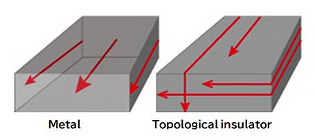
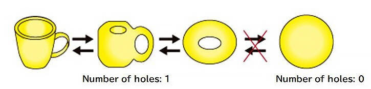
The "topological insulator" was proposed in 2005 (Fig. 1). It is a groundbreaking device that conducts electricity on its surface but not through its interior. Topology in mathematics is a geometrical concept that focuses on properties that do not change even if a shape is continuously changed (Fig. 2). The name "topology" is believed to have been used because the concept has also been applied to the electronic state of matter. Its existence was proved through after a few years of experiments and searching for topology-based materials became a new trend in condensed-matter physics.
Professor Masahito Ueda, who is with the Graduate School of Science, The University of Tokyo, will lead the research in the CREST Research Area, "Creation of Core Technology based on the Topological Materials Science for Innovative Devices". Properties that were not possible to achieve with conventional materials can be realized with materials characterized based on the concept of topology. He says, "We will also create innovative devices with features such as miniaturization, high speed, low power consumption, and toughness, and we aim to realize an ultra-smart society."
Research institutes in Europe, United States, and China, which are competitors, are also investing substantially in development of these products. "CREST has gathered world-leading, top-class researchers across fields ranging from theory to practical application. Lively discussions take place every day," says Professor Ueda. Research Area Advisors also provide highly specialized advice to support overall area management. It is also a field where several concepts remain unclarified, and expectations for results are high.
Aiming for diamagnetic memory, but issues with magnetization and practical use remain.
One of the CREST research teams is led by Professor Satoru Nakatsuji, who is with the Graduate School of Science, The University of Tokyo, Institute for Solid-State Physics. He specializes in condensed-matter physics and is working on the development of magnetic materials with new functions and the clarification of the mechanisms of these materials.
Electrons have two important properties: electric charge, which is the source of electricity, and spin, which is the source of magnetism. Prof. Nakatsuji is addressing the challenge of developing unprecedented high-performance and low-power-consumption devices that exploit the properties of spin in electronics and can enable computational processing using electric charge.
Spin is the rotational motion of electrons and is of two types--upward and downward. A magnetic material with the same spin direction and with magnetization as strong as that of a magnet is called a "ferromagnet." In contrast, a magnet having spins in opposite directions and a magnetization close to zero is called an "antiferromagnet." A hard disk drive (HDD), which is a typical example of the application of spintronics, reads and writes information by controlling the direction of electron spin. Magnetic memory is regarded to be non-volatile because it can store information without an external electricity supply and ferromagnets, such as cobalt-iron alloys, have been used for this purpose.
Meanwhile, it is known that using an antiferromagnet instead of a ferromagnet increases the spin response speed by two to three orders of magnitude. In addition to this, in the case of antiferromagnets, the spins are oriented in opposite directions, meaning that there are no concerns regarding leakage flux being generated, unlike for a ferromagnet. Moreover, faster reading and writing are possible. Antiferromagnets are expected to be applicable in large-capacity magnetic memory. However, because antiferromagnets have almost no magnetization, it is difficult to read and write information using the spin direction. This has resulted in them not being used in practical applications.
Anomalous electromotive force in manganese compounds. Discovery of the effect of a fictitious magnetic field.
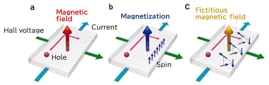
In contrast, Professor Nakatsuji discovered in 2015 that an antiferromagnet in the form of the manganese and tin compound Mn3Sn exhibits an "anomalous Hall effect," which is comparable to a ferromagnet at room temperature (Fig. 3). When a current flows through a substance, an electromotive force is generated in the direction perpendicular to the magnetic field and current. This is called the "Hall effect." This occurs because when a magnetic field and an electric current are perpendicular to each other, the direction of movement of the electrons flowing as an electric current is bent by the magnetic field. Meanwhile, in the case of ferromagnets, which possess magnetization, the Hall effect occurs even if a magnetic field is not externally applied. This phenomenon is called the "anomalous Hall effect."
It was also found in 2017 that Mn3Sn presents a "magnetic thermoelectric effect." Unlike conventional thermoelectric conversion, the magnetic thermoelectric effect is a phenomenon in which an electromotive force is generated in the direction perpendicular to the magnetic field/temperature difference. In the past, it was believed that only a ferromagnet with strong magnetization can generate a practically usable thermoelectromotive force. However, it has been discovered that even ferromagnetic Mn3Sn with small magnetization can produce a thermoelectromotive force as large as that of a ferromagnet.
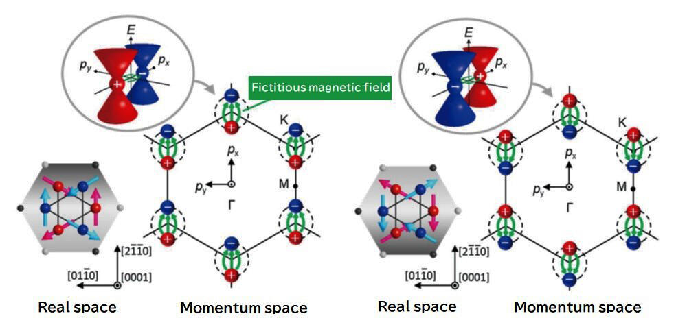
In subsequent studies, Professor Nakatsuji and others found that these effects originate from the topology of matter. "In fact, one of the most well-known topological materials has been theoretically predicted to be a new type of magnetic material in which Weyl particles, which have been studied in the field of elementary particles, are responsible for magnetism and conduction." It is known that Weyl magnets generate a large fictitious magnetic field equivalent to 100-1,000 Tesla when converted to real space. "Mn3Sn was the first substance to be identified as a Weyl magnet, and its anomalous Hall effect originates from the fictitious magnetic field generated by the Weyl particle," says Professor Nakatsuji (Fig. 4).
Previous studies have described how Weyl particles can be controlled using a magnetic field; however, their control using an electric current has not been reported. By contrast, in April 2008, Professor Nakatsuji and others created a substance consisting of a multilayer film of Mn3Sn and non-magnetic metals, namely platinum and tungsten, and succeeded in controlling it with an electric current (Fig. 5).
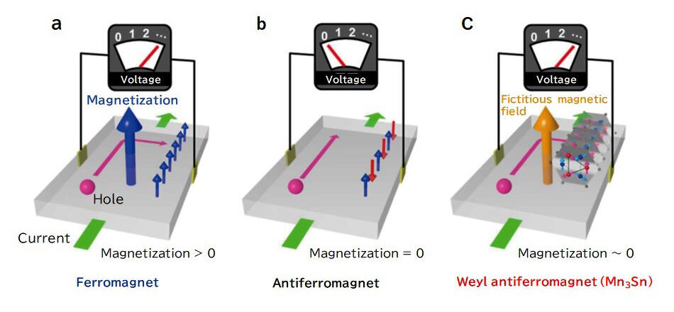
In general, the anomalous Hall effect increases in proportion to the magnitude of magnetization (a).
Given that the magnetization of an antiferromagnet is zero or very small, it is difficult to measure the anonymous Hall effect (b).
In the Weyl antiferromagnet Mn3Sn, owing to the effect of the fictitious magnetic field created by a Weyl point, an anomalous Hall effect comparable to that of ferromagnets appears even if the magnetization is very small (c).
"This achievement was a major step toward the practical application of ultra-high-speed, large-capacity non-volatile magnetic memory using topological materials," he said.
Inexpensive iron material provides magnetic thermoelectric effect at room temperature with no magnetic field.
In addition, Professor Nakatsuji and his research associates have been searching for topological materials that exhibit a high magnetic thermoelectric effect at room temperature. In April 2008, they discovered that the iron-aluminum alloy Fe3Al and iron-gallium alloy Fe3Ga are about 20 times more potent than iron alone (Fig. 6). "Topological materials cannot be discovered by blindly synthesizing compounds. Using computational science, we focused on iron materials that are inexpensive and industrially easy to use," recalls Professor Nakatsuji. It was also clarified that these phenomena originate from the topological electron band structure called nodal lines.
The "Seebeck effect" involves an electromotive force being generated by applying a temperature difference between the two ends of a substance. Thus, the module structure becomes complicated because the electromotive force is generated in the same direction as that of the temperature difference. Meanwhile, in the case of the magnetic thermoelectric effect, an electromotive force is generated in the direction perpendicular to that of the temperature difference and magnetization, and the direction of power generation can be controlled by the direction of the magnetization. Hence, a large-area thin film can be developed using printing technology to fabricate a non-bonded modular structure (Fig. 7).
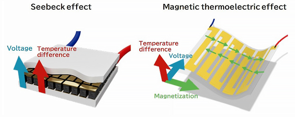
Non-junction flexible thermoelectric conversion module based on the magnetic thermoelectric effect (right).
In recent years, ignition due to temperature rise has become an issue for lithium-ion batteries. To combat this, the development of heat-flow sensors that exploit the properties of metals that easily transfer heat is being considered. "By sensing the heat flow using sensor, we can detect abnormalities in chemical reactions." "We believe that can we not only prevent ignition but also extend the lifetime of batteries." "We aim to put these sensors to practical use as soon as possible," says Professor Nakatsuji.
Adapted to optical integrated circuits by utilizing circularly polarized light and optical vortices.
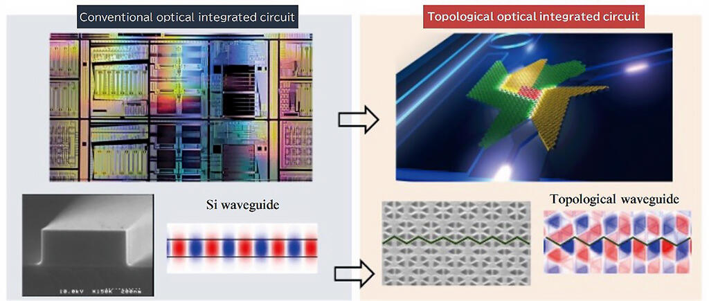
Under the direction of Principal Investigator Xiao Hu, who is with the National Institute for Materials Science, International Center for Materials Nanoarchitectonics, research on the photonics field has been conducted by Assistant Professor Tomohiro Amemiya, who is with the Tokyo Institute of Technology. Professor Amemiya, who specializes in optical communication, is developing an optical integrated circuit that can process a large amount of data at high speed by using topology. In today's information-oriented society, optical fibers are used for data transmission, but semiconductor optical integrated circuits are responsible for transmitting and receiving information at both ends. This is one of the core technologies that supports modern society, as it provides the necessary functions by integrating innumerable optical elements in a single chip.
In conventional optical integrated circuits, information is controlled using the light intensity, phase, wavelength, and related properties. "By incorporating a topological structure into an optical integrated circuit, it becomes possible to handle information produced by the topology of light, such as circularly polarized light and optical vortices." "It is essential to make good use of this information in order to process larger amounts of data at high speed," says Professor Amemiya (Fig. 8). Based on Professor Hu's theory, the objective is to introduce a microstructure developed by combining triangles (a topological structure) into an optical circuit, and to control the topological information on a chip.
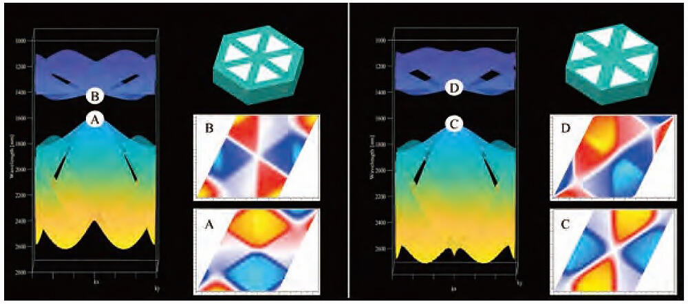
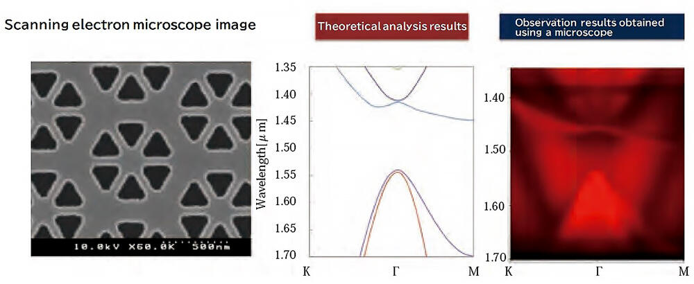
The photonic band diagram is an important indicator that determines the characteristics of optical materials with topological structures (Fig. 9). By evaluating this, it is possible to predict optical phenomena in the structure to some extent. In conventional photonic band diagram measurement, light is produced from a specific direction, and its transmission and reflection characteristics are evaluated. However, this method requires an optical system that matches the sample, and the process from presetting to measurement requires considerable time. "In manufacturing, the cycle of fabrication, evaluation, and enhancement is critical." "Every year, new students enroll in the university, so we needed an evaluation device that anyone could use to obtain immediate results," emphasizes Professor Amemiya.
Development of evaluation equipment in collaboration with companies with cost reductions using existing technology
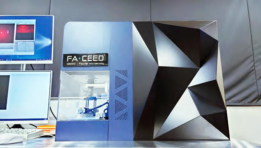
Professor Amemiya realized that if this was a device that he needed, then others would probably need it as well. He embarked on the development of a photonic band diagram microscope with Tokyo Instruments (Edogawa-ku, Tokyo), which has a wealth of experience in developing equipment in collaboration with universities. The design was based on the reconstruction of the band diagram by illuminating the sample with light at various wavelengths and observing the Fourier image of the scattered light. "Only the algorithm was newly conceived; the device itself was developed by combining existing technologies." "Thanks to that, we were able to create a device of stable quality without much cost or time investment," Professor Amemiya said with a smile.
The completed device has been on sale since June 2021 under the product name "FA-CEED." One of its features is that it is simple and fast (Fig. 10). By simply setting the sample in the holder, data can be automatically obtained in a short time. When they actually observed the band diagram of the topological photonic material using "FA-CEED," they were able to obtain observation results that support the theoretical analysis (Fig. 11). Because of the improvement in experimental efficiency provided by this device, it could be possible to proceed with the task of efficiently incorporating this device into an optical integrated circuit by creating a topological structure with satisfactory yield.
Researchers have honed their expertise through their research to date, but Professor Nakatsuji emphasizes that cross-disciplinary work is essential to address completely new concepts. "It has become commonplace for students from different laboratories to discuss ideas each with other. In the future, researchers with a focus on various fields will play an active role in development."
Professor Amemiya also says that the project has expanded his academic mindset. "Because my field is different from that of Professor Hu, I had only spoken to him once at an academic conference before speaking to him about this project, and we had barely had any interactions." "Now, I have online meetings with him on a weekly basis, and I've learned a lot," he said.
Professor Ueda is confident that more results will follow if researchers cooperate with each other and a system that allows them to study comfortably is adopted. The possibilities of developing topological materials have expanded considerably, and their importance has increased. Professor Ueda and others are steadily paving the way for the realization of a super-smart society.