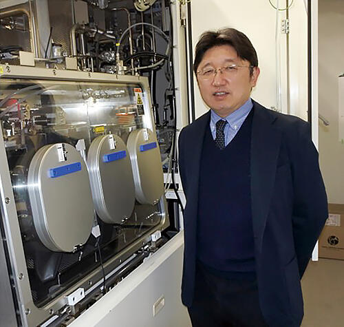
Professor, Faculty of Science and Technology, Meijo University
CREST Research Director since 2016
Laser diodes, which are compact, efficient and have low power consumption, are coherent light sources with controlled phases and wavelength. Infrared, red, green, and blue laser diodes have implemented to date, but in recent years there has been demand for laser diodes in the ultraviolet (UV) range, which has higher energy. Professor Motoaki Iwaya of the Faculty of Science and Technology, Meijo University, made excellent use of his own semiconductor technology and new methods, and invented the world's first UV-B laser diode. It is hoped that this outcome will pioneer new findings in advanced photonics, and lead to solutions to issues in a variety of fields - not just in industry, but also in chemistry, environmental issues, medicine and bioscience too.
Research that was started in the 1950s, taking on the challenge of one of the remaining unexplored fields
Laser is coherent light with uniform wavelength and phase, and has excellent directivity and convergence. They are used in products in a variety of fields, including optical discs, laser printers and optical communications, and are essential for everyday life. Among the different types of laser, laser diodes based on semiconductor materials have excellent properties when compared to gas and solid-state lasers. They are small and highly efficient, with a long life and high productivity, and so they are widely used.
The structure of a laser diode sees a layer known as the "active layer" sandwiched between an n-type semiconductor, in which the free electrons with negative charge are the majority carriers, and a p-type semiconductor, in which the free holes with a positive charge are the majority carriers (Figure 1). This structure is designed so that it confines the light and acts as an optical cavity that creates a standing wave of light. When voltage is applied to this structure, the high-energy free electrons in the n-type semiconductor and the free holes in the p-type semiconductor are injected into the active layer and recombine.
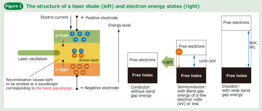
The energy generated by these particles recombining - in this case, the energy equivalent to the band gap energy of the material - is converted to photoelectricity and oscillates as a laser beam. Band gap energy is the energy range for which no electronic states can exist and is decided by the semiconductor material. The wider the band gap energy, the greater the oscillating light energy.
The idea for this technology was proposed in the 1950s, and full-fledged development began in the 60s. First, the light energy was small, i.e. in the long-wavelength, infrared range, then it was increased to the large-energy short-wavelength range, moving from red to green to blue (Figure 2). After this, there was demand for a laser diode with even higher energy, i.e., in the UV region. However, to achieve this, it is necessary to create a high-quality semiconductor material with a wide energy gap exceeding 3 eV, and to ensure laser oscillation by injecting a large electric current that will generate optical gain.
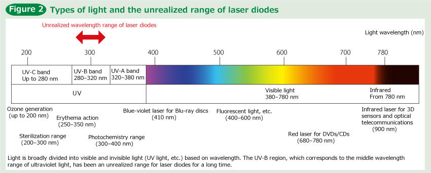
Researchers all over the world have competed to develop this, and a laser diode in the long-wavelength UV range of 320-380 nanometers (nm; nano = 1 billionth) was invented in 2003, with a laser diode in the short-wavelength UV range of less than 280 nm being created in 2019. Thus, the final unrealized range was a UV-B laser diode in the medium-wavelength range of 280-320 nm. This wavelength is well known as the cause of sunburn. It was Professor Motoaki Iwaya of the Faculty of Science and Technology, Meijo University, that took on this difficult challenge, leading research titled "Realization of deep UV semiconductor lasers and the study of ultra-high-concentration impurity and polarization semiconductors" in the "Advanced core technology for creation and practical utilization of innovative properties and functions based upon optics and photonics" research area of CREST.
Wavering determination after multiple failures: renewed efforts based on Dr. Akasaki's encouragement and reinforcement
Professor Iwaya was a student of Dr. Isamu Akasaki (d. 2021), who won the Nobel Prize in Physics in 2014 for "the invention of efficient blue light-emitting diodes which has enabled bright and energy-saving white light sources," and received his guidance for over 20 years, starting from his days as an undergraduate student. He says that Dr. Akasaki taught him many things, including how to think about technology and research, how to be prepared as a researcher, how to conceive and approach ideas, and how to adopt a perspective. "He looked over all my papers and gave me accurate advice and suggestions for each one. It's no exaggeration to say that if I hadn't met Dr. Akasaki, I would not have a career as a researcher."
Originally, the world of electronic solid-state engineering thought that it was probably impossible to develop the UV-B laser diode. The reasoning was that such a laser diode would need a semiconductor material with band gap energy of 3.8-4.4 eV, but materials that exceed 3 eV have highly insulating properties. In other words, researchers had to solve the paradox of pushing the large current required for laser oscillation through a material that does not conduct electricity. Moreover, to realize a laser diode that could withstand stable use, it was essential to develop new materials with high-quality crystals that have few defects.
Most researchers were constrained by the commonly held idea that it was impossible, and so they did not focus on this research. However, Professor Iwaya boldly decided to take on the challenge: "If I'm going to do something, I want to focus on a difficult problem that no one has been able to solve." Even so, although he used a variety of techniques and engaged in developing many different materials, he kept being rebuffed by the high hurdles required, and gradually his determination wavered.
Then, several years after he started, he informed Dr. Akasaki of his intent to finally abandon his research. Professor Iwaya recalled that when he did so, the normally gentle Doctor's demeanor completely changed, and he became very angry. "Is that the extent of your determination? You've involved many students, can you take responsibility for that? If this is what makes you give up, you should quit being a researcher." On that day, Professor Iwaya took up his challenge again.
Realizing the highest quality AlN: manufacturing an AlGaN layer with 3D growth
Professor Iwaya put out feelers in a variety of fields, built up every hypothesis he could think of, and tried many different techniques and material development. He and his group fabricated hundreds of test samples. After this, he engaged in repeated trial and error, and finally felt that he was beginning to get results four years after he restarted his work, in around 2014. Then in 2016, he was selected for CREST, and from this, several of his ideas have taken concrete forms. These are the three techniques of "high-temperature heat treatment of aluminum nitride (AlN) formed through sputtering," "creating high-quality aluminum gallium nitride (AlGaN) through 3D growth" and "polarization doping" (Figure 3).
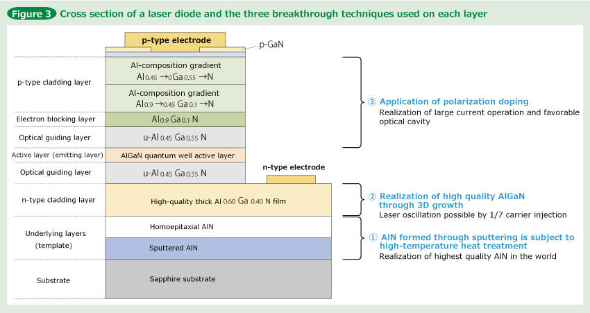
At first, a 2D crystal growth method was used for the n-type cladding layer, in order to form high-quality AlGaN crystals. However, numerous splits (cracks) and lattice defects (dislocations) formed during crystal growth, and Professor Iwaya was unable to obtain high-quality crystals that could withstand laser oscillation. Generally, cracks and dislocations lower the luminous efficiency, so the crystals did not reach the anticipated value of 210 kW/cm2, which is the threshold value for an optically pumped laser.
Conventionally, the substrate and the crystals grown above it must be consistent with the lattice constant - the axis length and angles. It is thought that it is not possible to obtain high-quality crystals if there is a lattice mismatch that exceeds 1%. When he was developing blue LEDs, Dr. Akasaki faced this same problem, and to overcome it he developed a low-temperature deposited buffer layer technique. This technique involves growing gallium nitride (GaN) crystal after depositing AlN on the sapphire substrate. With this, he obtained flat GaN crystals with very few crystal defects, leading to the invention of blue LEDs.
It was rare to use 3D growing methods in AlGaN materials research, but Professor Iwaya possessed the knowhow, and followed Dr. Akasaki's method to begin forming crystals. He used a high-quality AlN formation technique developed by Professor Hideto Miyake of the Graduate School of Regional Innovation Studies, Mie University, who was a joint researcher on this project. This technique has recently been widely used to fabricate AlN templates for UV LEDs.
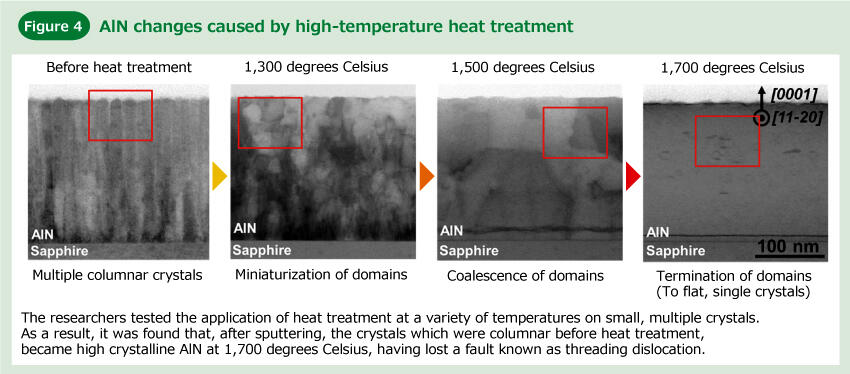
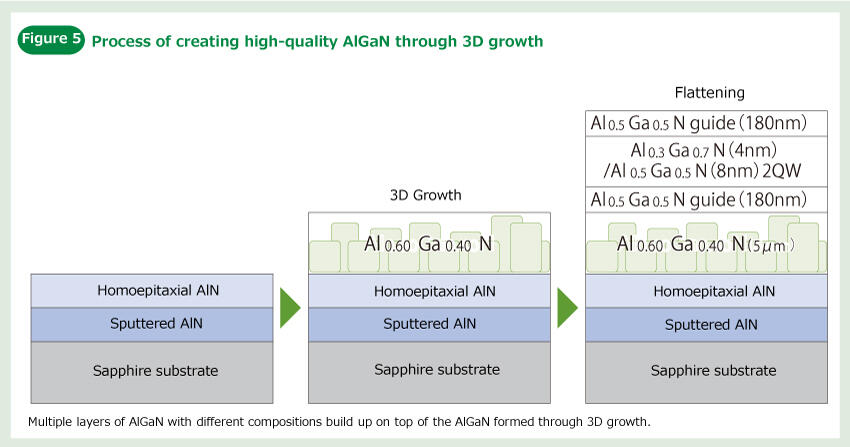
Ions such as nitrogen collide with AlN, which serves as the raw material, and a thin AlN film is deposited above the sapphire substrate through a sputtering technique that causes the molecules that have been pushed away to stick to the substrate. The manufactured crystals are layered in a microcrystalline state. The Professor succeeded in obtaining a high crystalline AlN film with very few crystal defects by subjecting them to high-temperature heat treatment at 1,700 degrees Celsius (Figure 4). Using this AlN as a template, he engaged in 3D growth of AlGaN on top of it (Figure 5). As there was a large lattice mismatch of over 1% between AlN and AlGaN, things weren't straightforward, and he tested various conditions. "Development took around three years, but thanks to my students' great efforts, we lowered the optically pumped laser threshold power density to 36 kW/cm2, equivalent to around 1/7 of that for 2D growth," he said, smiling. They have now established a method to reduce this even further - by around half.
Introducing insulation engineering techniques: successful oscillation using polarization doping
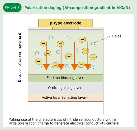
The crystals that everyone had worked hard to form would come to nothing without laser oscillation, but it is not easy to inject a large current into crystals with wide band gap energy. Moreover, a laser diode requires a film thickness greater than the light's wavelength to control the beam. In conventional semiconductor engineering, it is not possible to realize the large-current density operation needed for laser oscillation in cases of conductivity control through the addition of impurities, which is often used. Thus, Professor Iwaya focused on polarization doping.
Generally, semiconductor crystals are electrically neutral, but nitride semiconductors lack symmetry, so they possess a large polarization charge. Polarization doping is a technique that generates electrical conductivity carriers through the application of this polarization charge (Figure 6). Polarization is a concept used for insulating materials. A group from the University of Notre Dame in America announced that it is possible to generate free electrons and free holes by making use of the polarization effect and that they succeeded in improving the characteristics of blue LEDs.
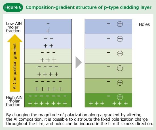
In this research, Professor Iwaya made use of polarization doping for the p-type cladding layer and altered the level of polarization in terms of the gradient by changing the composition of the AlGaN material (Figure 7). In so doing, he was able to ensure that the polarization fixed charge is distributed, and in 2019 he simultaneously realized a level of current injection that allows laser oscillation and the formation of an optical cavity. This technique was new to semiconductor engineering and allowed him to overcome the paradox of "running a current through a material that does not conduct electricity," which was previously said to be impossible to achieve.
Realization of deep UV semiconductor lasers and the study of ultra-high-concentration impurity and polarization semiconductors.
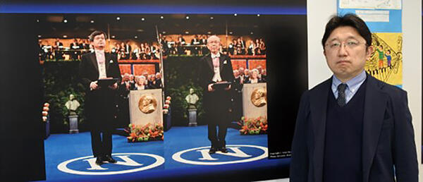
Professor Iwaya standing next to a photo panel of the award ceremony for the Nobel Prize in Physics in 2014 (Dr. Akasaki is on the right, and Special Professor Hiroshi Amano of Nagoya University is on the left).
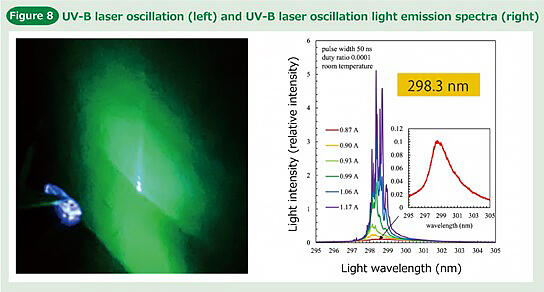
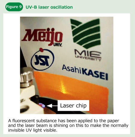
When a test device created using these three techniques was evaluated at room temperature, it was confirmed that it had the light emission pattern and spectra characteristic of laser diodes (Figures 8 and 9). With this result, in February 2020 it was announced that the world's first UV-B laser diode had been invented. Professor Iwaya looks back at the many exchanges with the peer review committee before the paper was published. "Because it was the first time in the world, it was natural that they would want to ask if I'd really managed it. I submitted a lot of materials for evidence, and I was thrilled when it was finally acknowledged."
There was a huge stir as soon as this invention was announced, in Japan and overseas. The development of this innovative semiconductor device was praised as an extremely important result in the study of crystal growth, as well as in the evolution of semiconductor engineering, and dominated academic conferences and newspapers. It also lit up the future of optical science and semiconductor engineering.
100th the size and electricity consumption: working toward DNA sequencing analysis and skin treatment
This newly developed laser diode has applications in a wide range of fields, meaning that its impact is huge. Compared to gas lasers and solid-state lasers used in the same wavelength range, it is extremely compact, has lower electricity consumption, a longer life span, and costs less. Normal gas lasers are around 1-2 meters in size, but this laser diode is around 1 cm, 1/100 of the size. Its electricity consumption is also around 1/100 of gas laser electricity consumption, and its life is approximately 100-fold longer, from around 100 hours to 10,000 hours.
If this can be mass-produced, it is hoped that prices will drop to less than 1/100,000 of a gas laser. "Looking at history, it is clear that a single discovery can change the world in one go. If devices that use this laser are popularized, we will be able to explore a world previously unseen," emphasized Professor Iwaya. In the medical and bioscience fields, there is the major possibility of realizing research and medical treatments that were not possible with lasers of other wavelengths, including skin treatments and DNA sequencers that analyze DNA base sequences.
Moreover, if researchers can change crystal composition, it may be possible to create laser beams of all wavelengths in the medium-wavelength range, and joint research is already going ahead with universities and companies in Japan and overseas. Professor Iwaya is leading this research and spends his days focusing on research that will lead to further technological innovation, with an eye to the next era. When he does so, there is a motto that he always remembers. "A result that rewrites the textbooks is the best research." These are the words of the late Dr. Akasaki. (Text: Kazuyuki Katayanagi; photos provided by Meijo University)
(Text: Kazuyuki Katayanagi; photos provided by Meijo University)