Power semiconductors using silicon carbide (SiC) are seeing increased use as a method of achieving carbon neutrality through their ability to conserve energy and use it more efficiently. Professor Tsunenobu Kimoto of the Graduate School of Engineering, Kyoto University, has established a fundamental technology that significantly reduces defects at the oxide film/SiC interface, a long-standing area of difficulty in the field of SiC power semiconductors. The technology simultaneously achieves reduced costs, high reliability, and significant performance improvements. His team has also demonstrated basic operations of integrated circuits using SiC semiconductors at high temperatures, paving the way for their use in various environments.
Industry-University Consortium aiming for the fusion of scientific research and advanced technology
In January 2016, the Japanese government proposed "Society 5.0" as a vision of the future society that Japan should aspire to. This is a new human-centered society following the hunting society (Society 1.0), agricultural society (Society 2.0), industrial society (Society 3.0), and information society (Society 4.0). The goal is to create unprecedented new value through the sharing of knowledge and information, and to achieve economic development and solve social issues.
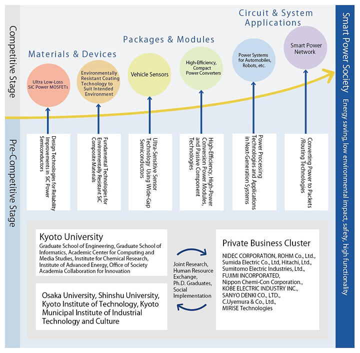
In January 2019, Kyoto University launched the OPERA Consortium for Co-Creation of Super Smart Energy Societal Infrastructure Technologies (Figure 1). The Consortium works to develop innovative semiconductor technologies to realize Society 5.0 and a future society with extreme energy conservation and low environmental impacts while being safe and highly functional. Professor Kimoto heads this area. The Consortium aims to fuse academic and scientific research, which is the key to innovative creation, advanced universal technologies, and fostering future generations of researchers.
Figure 1: Overview of OPERA Consortium for Co-Creation of Super Smart Energy Societal Infrastructure Technologies
To achieve a high level of international competitiveness in the field of semiconductors, it is vital to develop R&D not only for devices but also for peripheral equipment while leveraging technological advantages. Professor Kimoto explained, "Consortium participants cooperate in R&D in non-competitive areas in the initial stages. Then, when commercialization becomes feasible, they develop them into separate joint research projects in competitive areas."
The Consortium also collaborates with the Kyoto University Open Innovation Institute, which plans and implements large-scale joint research, as well as with Kyoto Prefectural and Kyoto Municipal governments to innovate in smart energy with the local community. One example of this collaboration is providing technical guidance to local companies developing energy-saving and high-efficiency energy utilization technologies.
Six technology themes that are vital to solving related problems were established to fuse them with scientific research, which holds the key to producing innovation and universal advanced technologies. The themes include Design Technologies for Reliability Improvements in SiC Power Semiconductors, Fundamental Technologies for Environmentally Resistant SiC Composites, Ultra-Sensitive Sensor Technologies Using Wide-Gap Semiconductors, High-Efficiency, High-Power Conversion Power Modules, and Passive Component Technologies, Power Processing Technologies and Applications in Next Generation Systems, Converting Power to Packets/Routing Technologies.
Of these themes, Design Technologies for Reliability Improvements in SiC Power Semiconductors, led by Professor Kimoto, has produced two research results that will lead to energy innovations through innovative semiconductor technologies. Two long-standing challenges included improving the performance of SiC power semiconductors (transistors) by forming non-oxidized oxide films and demonstrating the basic operation of low-power consumption integrated circuits at 350℃.
Figure 2: Comparison of Si and SiC properties
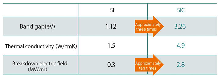
Si is reaching its theoretical limits - SiC provides a breakdown electric field that is 10 times higher
Solving the energy crisis is one of the most critical challenges of this century. However, establishing technologies that use energy efficiently is just as crucial as using renewable energy. Semiconductor power devices are essential to efficient energy use. They are used in all electronic devices with power circuits, from home appliances to solar power generation and electric vehicles, and are a familiar component that supports our daily lives.
Semiconductor power devices mainly use silicon (Si), but Professor Kimoto points out that silicon device performance is reaching its theoretical limit. "New semiconductor materials will be essential in the near future. The most promising of these is silicon carbide (SiC), a silicon and carbon compound." Silicon carbide is superior to silicon because it has a breakdown electric field (one of the indicators of material strength) that is 10 times higher and has three times the energy band gap, a determiner of the upper operating temperature limit. In addition, large-diameter, high-quality wafers with a diameter of 150 mm are now widely available and are expected to be used as a material for power devices that transcend the limits of silicon since the p- and n-types required for device fabrication can be controlled over a wide range (Figure 2).
Companies worldwide began full-scale research and development of SiC power semiconductors around 1998, and the mass production of SiC diodes began in 2001, followed by SiC transistors in 2010. Starting with power supplies for workstations and other equipment, they are now used in air conditioners, power regulators for solar power generation, fast chargers, industrial motors, and other power systems. Railcars and electric vehicles equipped with SiC power semiconductors have also become a significant topic of conversation.
Making oxide film without oxidation
Reducing defects through an entirely new concept
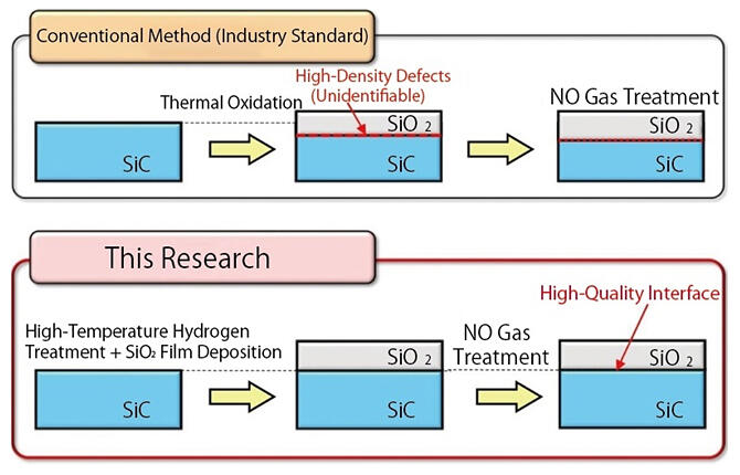
The most fundamental and essential transistors in Si power semiconductors are metal-oxide-semiconductor field-effect transistors (MOSFET). The heart of these transistors is the joint interface between the SiO2 oxide film formed by the silicon surface's thermal oxidation and the silicon. In SiC MOSFETs, a gate oxide (SiO2) film can be formed on the surface by thermal oxidation of SiC. However, in doing so, defects more than 100 times in density greater than those of Si are generated at the joint interface between the oxide film and SiC, significantly limiting device performance. Researchers have been trying to reduce these defects for more than 20 years, but little progress has been made. However, Professor Kimoto and his team have successfully reduced them through the unexpected concept of forming oxide film without oxidation.
Associate Professor Yuichiro Matsushita of the School of Materials Science and Informatics, Tokyo Institute of Technology, has discovered through first-principle calculations that thermal oxidation of SiC always results in the formation of a high density of defects, which are caused by carbon atoms at the interface.
Based on the results of these calculations, the team conducted a series of experiments and theoretical considerations and found that several processes effectively reduced defects. One is removing any remaining defects on the SiC wafer surface using hydrogen etching before forming an oxide film and then depositing SiO2 on the substrate surface using a chemical vapor deposition (CVD) method. The idea is that forming a high-quality oxide film on the SiC surface will prevent new high-density defects from being generated during oxide film formation.
Furthermore, after the oxide film is deposited, interface nitridation is performed using nitric oxide (NO) gas to improve the quality of the interface (Figure 3). These efforts enabled the new device to achieve higher quality, reducing defects to about one-fifth of the conventional worldwide standard. In addition, the channel mobility, which expresses the mobility of carriers, has also been doubled.
Figure 3: The Newly Proposed SiO2 / SiC Fabrication Method
Fine trench structure increases channel mobility by six to eighty times
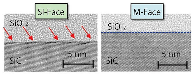
Professor Kimoto and his colleagues continued to further improve performance. The chip structure was changed from the conventional planar-type, in which the gate electrodes are attached to the wafer surface, to a trench-type, in which the gate electrodes are embedded in micro trenches on the surface, and oxide films were formed on the A and M faces, which are vertical to the Si face, (0001), on the wafer surface (Figure 4 and Figure 5). This method improves channel mobility by six to seven times compared to the conventional method.
Figure 4: Cross-Section View of a Trench-Type MOSFET
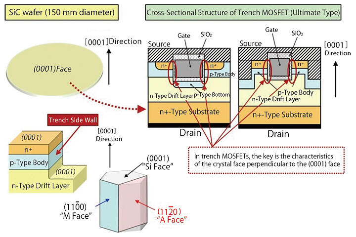
Figure 5: Electron Microscope Image of SiC MOS Interface
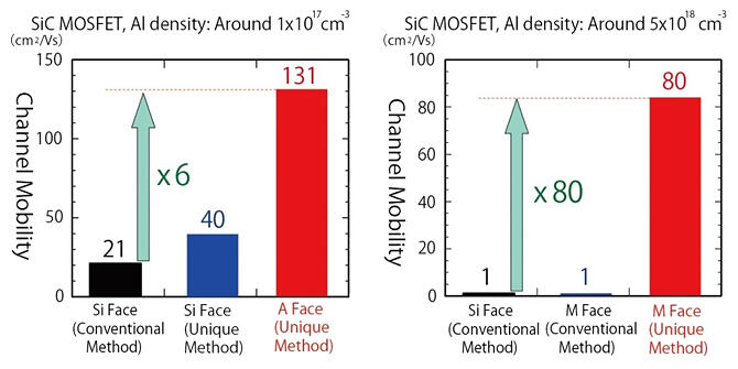
As in SiC transistors that are actually manufactured, p-Type regions with relatively high concentrations of aluminum, an acceptor-type impurity, were formed to fabricate MOSFETs on the A and M faces. As a result, channel mobility was improved by six to eighty times compared to the conventional method (Figure 6). This method dramatically improves reliability and reduces costs to about one-third of conventional methods by reducing the chip area.
Figure 6: Comparison of Channel Mobility
In his 30 years of research, Professor Kimoto said he was always troubled by defects at the interface between the oxide film and SiC. "We'd made more than 100 hypotheses, but they all failed. We were still groping around in the dark. This is the first time the true nature of the problem has come to light, and I believe we have achieved a fundamental solution." he said, smiling. The global market for SiC power semiconductors is approximately 120 billion yen. However, the market is expected to increase to 300 to 600 billion yen in the next five years. Increased practical applications of SiC power semiconductors will significantly contribute to energy conservation in society.
Basic operation successfully demonstrated at 350℃: Power consumption of 1/10,000 current levels may be possible
In recent years, there has been a growing trend toward extending the range of applications of integrated circuits to high-temperature environments inaccessible to humans. In oil and gas drilling operations, ground information must be sensed in real-time with underground temperatures of over 300℃. In planetary exploration, for example, the pressure on the surface of Venus is about 70 atmospheres, and the temperature is over 400℃, making it difficult for probes to land. In addition, the combustion chambers of aircraft and automobile engines can reach temperatures up to 600℃. Despite this, fine control of fuel mixture ratios is required in these environments.
Currently, mainstream Si semiconductors malfunction at about 250℃, making it theoretically impossible to use them in these high-temperature environments. However, SiC devices are attracting attention because of their ability to operate normally at temperatures up to about 800℃. "SiC MOSFETs have a temperature limit of 250 to 300℃ due to the oxide film contained within them. They're also vulnerable to radiation. These factors make stable operation under extreme conditions difficult," says Professor Kimoto.
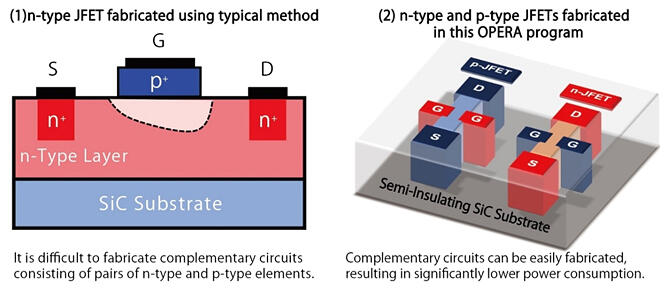
This has brought the junction-type field-effect transistor (SiC JFET) with p-n junctions into the spotlight. Their lack of oxide film makes them a promising transistor for SiC integrated circuits operating at high temperatures. However, JFETs fabricated using conventional methods cannot form complementary circuits and require large amounts of standby power. In high-temperature environments of 300℃ or higher, where SiC integrated circuits are expected to see use, power is also expected to be limited, so low power consumption has been a significant challenge.
Typical JFET fabrication methods allow either n-type or p-type JFETs to be fabricated. However, Professor Kimoto, together with Assistant Professor Mitsuaki Kaneko of the same laboratory, succeeded in creating n- and p-type JFETs on the same substrate by implanting ionized atoms into the semiconductor by accelerating and colliding them with high voltage to fabricate devices using the ion implantation method. Ion implantation is a technology widely used in industry and is promising from the viewpoint of mass production.
Furthermore, for the practical production of integrated circuits, it is necessary to configure complementary circuits to reduce standby power. A normally-off characteristic, in which no current flows in the transistor when no voltage is applied to the gate, is essential for this purpose. Although it was considered difficult to achieve with conventional manufacturing methods, by sandwiching the JFET channel region from both sides and creating a structure with two gates, a normally-off characteristic was achieved, reducing standby power (Figure 7). "The complementary JFETs we have fabricated have operated consistently in our desired temperature range of room temperature to 350℃, with a standby power consumption of less than a few tens of nanowatts at most," he said with pride.
Compared to circuits using JFETs proposed overseas, the power consumption is said to be less than 1/10,000 of that of circuits using JFETs, which is undoubtedly a significant step toward practical application. It should be noted that circuits can be fabricated using standard processes for SiC semiconductors, which have a market in a different field from that of integrated circuits. Looking to the future, Professor Kimoto said, "Further basic research is needed to determine whether miniaturization, higher speed, and higher functionality are possible in JFETs, and we will continue studying them."
Figure 7: JFET Schematic