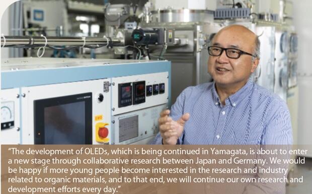
There is a measuring device called a "near-infrared (NIR) spectroscopic analyzer." To analyze the composition and properties of a target substance, the device irradiates light in the NIR region (which has a wavelength slightly longer than that of visible light) onto the substance and records the degree of absorption of each wavelength. Researchers from Japan and Germany have been working jointly for approximately three and a half years to improve the analytical capabilities of the spectroscopic analyzer and to make it more compact and affordable. Distinguished Research Professor Junji Kido of the Graduate School of Organic Materials Science at Yamagata University, a leading researcher in the field of organic electroluminescence, has proposed an organic electroluminescent device (OLED)-based light source that emits light in the NIR region and is promoting the development of a demonstration unit of the device combined with an organic spectroscopic sensor made in Germany.
More multilateral-analysis than existing light-emitting diodes (LEDs): Light intensity and lifetime are issues that must be addressed for practical application
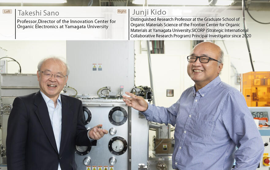
The development of an NIR spectroscopic analyzer was undertaken by Distinguished Research Professor Junji Kido and Associate Professor Hisahiro Sasabe of the Graduate School of Organic Materials Science, Frontier Center for Organic Materials and Professor Takeshi Sano Director of the Innovation Center for Organic Electronics at Yamagata University. Spectroscopic analyzers have long been used for various practical applications. One example is the pulse oximeter, which measures oxygen saturation in the blood and is still fresh in our memory for being used to assess the severity of COVID-19 infections and monitor the disease progress during medical treatment. Hence, what is the difference between this device and the NIR spectroscopic analyzer that Kido and his team are developing?
First, a description of the mechanism of the NIR spectroscopic analyzer.
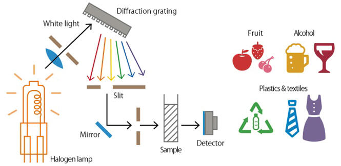
NIR rays are electromagnetic waves with wavelengths between those of visible light and thermosensitive infrared rays. The wavelengths typically range from 700 to 2500 nanometers. When a substance is irradiated with light in this range, only specific wavelengths corresponding to the composition and properties of the substance are absorbed within the substance. In a spectroscopic analyzer, light in the NIR region is emitted from a light source, and the degree of absorption of each wavelength by the test substance is detected by a sensor. The composition and properties of the substance are analyzed based on these results. The light source and sensor are the two crucial components of the spectroscopic analyzer.
One of the distinctive features of the spectroscopic analyzer developed by Kido is this "light source." Whereas red LEDs are used in pulse oximeters, Kido has found advantages in introducing an organic electroluminescent device. "Both emit light in the NIR region; however, the light emitted by LEDs is a single wavelength, whereas the light emitted by the OLED spans multiple wavelengths. This allows for substances to be analyzed multilaterally, which greatly improves our analytical capabilities." This high capability can be utilized in the analysis of materials (Figure 1).
Figure 1:Example of near-infrared spectroscopic analysis
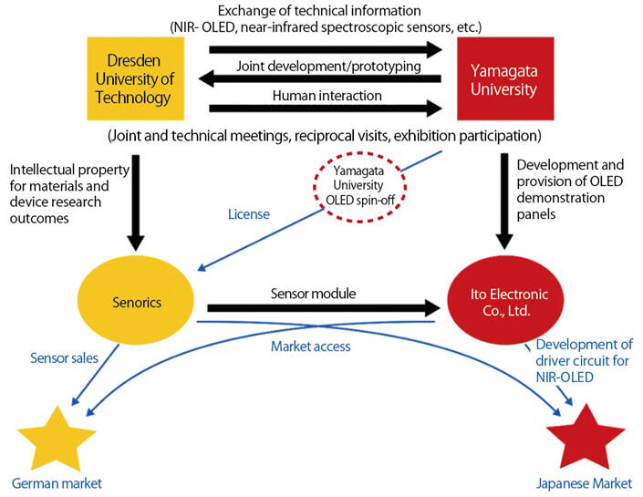
Additionally, using an OLED as the light source facilitates the miniaturization of the spectroscopic analyzer. There is a limit to the miniaturization of existing spectroscopic analyzers with high analytical performance as they mainly use halogen lamps as their light source. Because OLEDs are extremely thin, they obviate the limitations associated with the three-dimensional size of the light source. The greatest challenge in adopting OLEDs was whether they could emit light with sufficient intensity up to long wavelengths beyond 700−1000 nm in the NIR region. With regard to practical applications, both the intensity of the light and its long lifetime need to be ensured. To address this challenge of developing a new NIR spectroscopic analyzer using an OLED as the light source, Kido was selected for the JST (Japan Science and Technology Agency) SICORP program, "Development of miniaturized full-organic spectroscopic NIR-OLED sensor systems." This program promotes collaborative research between Japan and Germany, which is the country of Kido's research partners. The Japanese team consists of researchers from both Yamagata University and Ito Electronic Co., Ltd. (a local semiconductor product manufacturer in Sagae City, Yamagata Prefecture), and the German team is composed of scientists from both the Dresden University of Technology and Senorics GmbH (a university-launched venture company) (Figure 2).
Figure 2:SICORP organizational chart
A thin light source of 2 mm thickness: Low cost and high reactivity are also advantages
Professor Karl Leo of the Dresden University of Technology is a long-time acquaintance of Professor Kido. Although their areas of expertise are different, Professor Leo, like Kido, is a leading expert in OLED research. Germany had extended an invitation to Japan for the joint development of an NIR spectroscopic analyzer. Kido pointed out that the transition of OLED development in Japan and the uniqueness of Yamagata University are the background to the German team seeking Japan's OLED technology. "As OLED displays have become more widespread both in Japan and abroad, the role expected for universities is becoming more limited. In this context, Yamagata University's persistent efforts in challenging technological development may have been appreciated."
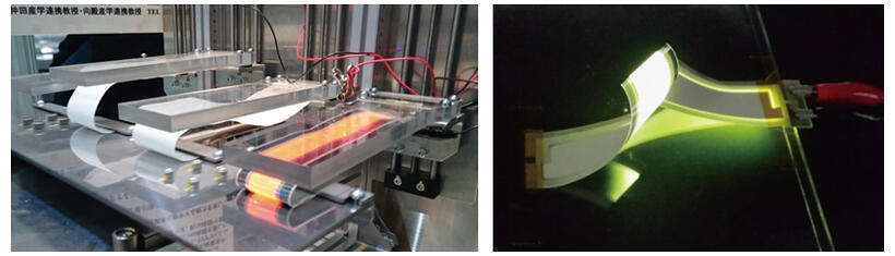
The symbolic technological development is the technique of organic electroluminescent material formation. This innovative idea of forming organic electroluminescent elements on flexible substrates can transform wallpaper into illuminations or displays (Figure 3). Furthermore, the current development of a film deposition technique based on a coating process is expected to reduce the cost of film deposition, as it requires much lower capital investment costs than those of conventional film deposition using the vacuum evaporation technique. While the development of this new film-coating deposition technique was underway, the university was approached by the German team to conduct collaborative research. "I was convinced that this was an excellent opportunity that would lead to the revival of Japanese manufacturing, and I accepted the invitation without hesitation," Kido recalled.
Figure 3:Flexible lighting panel fabricated with an OLED film deposition technique
The Japanese team possesses the technology to develop an OLED-based light source that emits red to NIR light, whereas the German team possesses the technology to develop a sensor that detects NIR light using organic photodiodes. Applying the technologies from both countries, Ito Electronic Co., Ltd. undertook the development of the driving circuit, whereas Senorics GmbH took on the development of an organic spectroscopic sensor and the final spectroscopic analyzer. The aim is to create an extremely compact spectroscopic analyzer consisting of a thin 2-mm-thick light source and a spectroscopic sensor of approximately the same thickness. While striving to attain the long lifetime, low cost, and high reactivity of organic electroluminescent elements as light sources to enable immediate startup and measurement, the research team aims to achieve a technical demonstration of the NIR-OLED at an exhibition scheduled for March 2024 in Germany.
Kido first began analyzing materials to overcome the OLED issues mentioned above. To attain the goal, it was necessary to develop devices that emit light with sufficient intensity in the NIR region of 700−1000 nm. A wavelength of approximately 770−900 nm was set as the initial benchmark. Although the theoretical possibility had already been supported by academic papers, the theoretical values of light efficiency and lifetime were insufficient to make their practical application as actual values worthwhile.
A sensitizer as a third component: Six times higher efficiency than conventional devices achieved
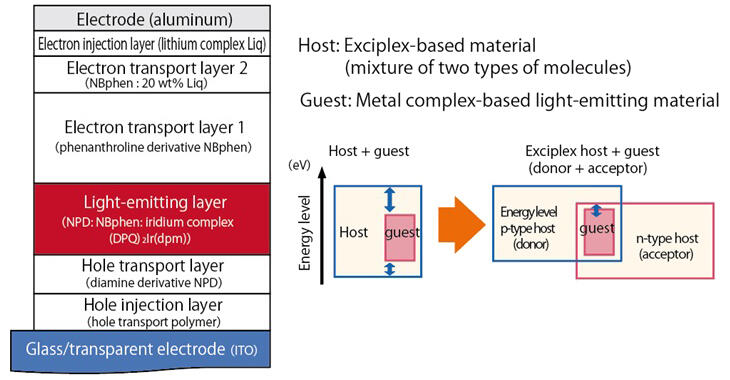
As part of his material analysis, Kido proceeded to select materials for the OLED and examine the device structure. "If one material lacks durability, it would cause deterioration in the overall device performance. The combination of materials needed to be optimized while taking into account their compatibility." The light-emitting layer, the heart of the OLED, is divided into two components, referred to as the "host" and "guest," respectively. The role of the guest is to emit light utilizing the charge sent by the host.
What materials should be used for the host and guest and how should they be constructed? After much trial and error, Kido applied the findings he had accumulated in the past to the selection of materials and structure of the device and successfully achieved optimization. One of his findings is the result of research using an OLED that emits deep red light close to the NIR region. First, an OLED with an emission wavelength range of 640−800 nm was prepared using an "exciplex-based" material which is a mixture of two types of molecules as the host and a "metal complex-based" light-emitting material as the guest. When the time required for the luminance to drop by half under a constant current density was measured, the lifetime significantly exceeded that of a conventional deep red OLED (Figure 4).
Figure 4:Organic EL light-emitting materials with the exciplex method
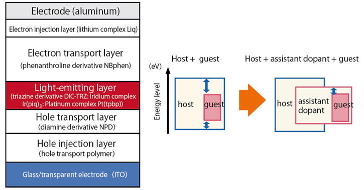
Having achieved this result, the attention was turned to phosphorescent materials that serve as sensitizers. The stepwise and efficient transfer of energy from the host to the guest of the light-emitting material was made possible with the "dopant-assisted" method, in which a third component is added between the host and guest. The light-emitting efficiency increased to approximately six times that of an OLED without phosphorescent materials added, and the time before the luminance decreases under high current density was extended, resulting in a longer lifetime (Figure 5). The observed emission wavelength range in the NIR region was 720−900 nm, with a peak at 770 nm. Kido said, "We could finally bring the wavelength range, intensity, and lifetime of the light to a level for practical use."
Figure 5:Organic EL light-emitting material using the dopant-assisted method
Tackling the final towering wall and looking toward the future beyond the demonstration unit
The joint research is arriving at a critical point in the realization of the final technology demonstration. The experiment conducted in Germany in September 2023 to combine the NIR-OLED and sensors was reproduced in Japan to determine if the same results would be obtained. As a result, discrepancies were observed. Sano, who was involved in the work, said, "We planned to measure alcohol concentration with the demonstration unit. When we measured a liquid that yielded a concentration of 30% in Germany, the results were different in Japan." He bemoaned the wall blocking his way forward.
As of October 2023, the cause of this problem is still under investigation. One possible reason is the influence of temperature. Infrared sensors used for detecting temperature tend to pick up heat. NIR spectroscopic analyzers are also affected by temperature. Kido pointed out a future challenge: "In addition to the heat generated inside the spectroscopic analyzer, there may be some influence from the external ambient temperature. In any case, we need to consider some form of heat dissipation measure."
Another problem is the difference between the emission and detection wavelength ranges. The emission wavelength range of the light source used by the Japanese team is a maximum of 900 nm, whereas the detection wavelength range of the sensor used by the German team is over 1000 nm. Kido speculates that this difference may be the cause of the discrepancy. One possible countermeasure is to bring the wavelength ranges used by the two teams closer to each other. If the NIR emission wavelength range can be widened to match the detection wavelength range of the sensor, there is a high possibility that the discrepancy can be reduced.
Since September 2023, the research teams have been working to improve the light-emitting element and are currently in the final stages of pushing toward an announcement. Expressing his hope and outlook, Kido said, "There must be many ways to use the device that we have not anticipated. If the results of the trial operation become widely known, people will ask, 'Can we use it in this way?' Such voices are important for future research and development." As the end of the research period approaches, Kido and Sano are looking even further ahead.
"The challenge of achieving flexible performance remains. We wish to not only realize the OLED as a light source but also eventually extend it to an organic photodiode as the sensor." The research team will take on the challenge of the practical implementation of a NIR spectroscopic analyzer that can be attached to curved surfaces, similar to the organic solar cells that are being developed in Japan and abroad. In the future, NIR spectroscopic analyzers are expected to play an active role in various fields, including material and food analyses. The future in which we can use them in our daily lives is gradually and steadily approaching.
(TEXT: Shunsuke Mogi; PHOTO: Hideki Ishihara)